
MOD-6 (Modulus-6) ripple counter – study & revision notes
In this post, we present a detailed write-up on MOD-6 (Modulus-6) ripple counter (study & revision notes).
We know that n-bit asynchronous counters can count N = 2n clock pulses, Where n = Number of Flip Flops. For example, a 3-bit counter has 8 different states (0 to 7) and it is a MOD-8 counter.
To count M clock pulses which is less than N (N = 2n), we need to take the help of a reset terminal (CLR) of the flip-flops. The combinational circuit (reset logic circuit) is designed in such a way that the output (Y) of this circuit must enable the CLR (reset) input of all the flip-flops to reset them after the count of M clock pulses.
Here is the state (sequence) diagram of the Mod-6 ripple counter (as shown in Figure 1).
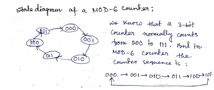
Figure 1: State sequence diagram of Mod-6 ripple counter.
The state diagram shows that the counter recycles after counting the value 101. So the combinational circuit is designed in such a way that the output (Y) of this circuit becomes 0 to enable the CLR (reset) input of all the flip-flops. That means after 6 clock pulses (or after counting 101) the counter output will be again 000. In the modulus-6 counter, there is a total of six states (0 to 5).
From the above diagram, it is clear that the minimum number of flip-flops (n) required to design a mod-6 counter is, M<2n 4<2n or n=3.
Here is the block diagram of the Mod-6 ripple counter (as shown in Figure 2).
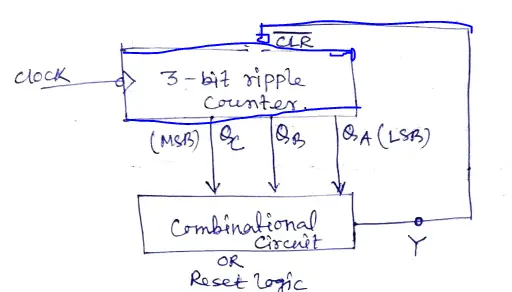
Figure 2: Block diagram of Mod-6 ripple counter.
From this diagram, it is clear that the combinational circuit has three inputs (QA, QB, and QC) and one output(Y) terminal. The output of the combinational circuit is further connected with the CLR (clear) input of all the Flip-flops. Now draw the truth table of ripple counter with the output of combinational circuit Y. Here is the truth table of a 3-bit UP counter (as shown in Table. 1)
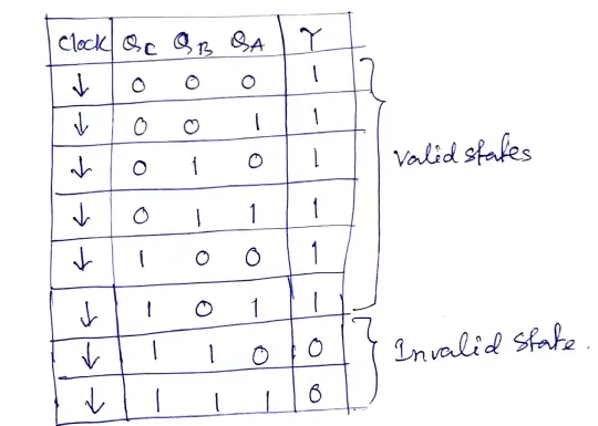
From this table, it is clear that the output of combinational (reset) logic circuit Y is equal to 1 for counts 0 to 5 (valid states) and it becomes 0 for count 6(which is an invalid state).
Now draw the K-map for the combinational circuit output Y, as shown in Figure. 3
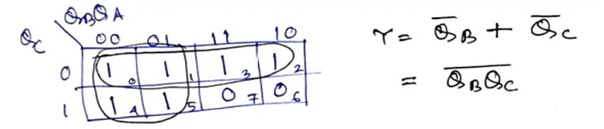
Figure 3: K-map for the reset logic circuit
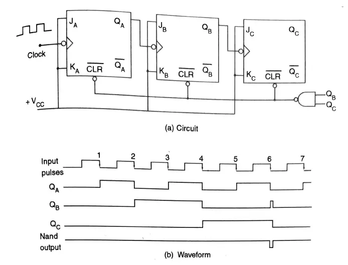
After solving the K-Map, finally, we have got the logic diagram of the Mod-6 ripple counter shown in figure 4(a). In this diagram, the 2-input NAND gate is part of the reset logic circuit.
The timing diagram of the Mod-6 ripple counter is also drawn as in figure 4 (b).
Related posts (for further study) on Binary Counter
Asynchronous Counter – study & revision notes
Synchronous Counter – Study & Revision Notes
How to design a Synchronous counter – step by step guide
2-bit Synchronous Binary Counter using J-K flip-flops
A 3-Bit Asynchronous Binary Counter – Up Counter
Asynchronous Up counter for Positive & Negative edge-triggered flip-flops
Binary Counter Sequential Circuit – FAQs
Frequently Asked Questions on Flip-Flops Sequential Circuit
Numerical problems on asynchronous counter & synchronous counter
J-K flip-flop – Frequently asked questions for semester & GATE exam
Modulus-M (MOD-M) asynchronous counter – Study and revision notes
Digital Electronics – Hub page
Author of this post
This post is co-authored by Professor Saraswati Saha, who is an assistant professor at RCCIIT, a renowned degree engineering college in India. Professor Saha teaches subjects related to digital electronics & microprocessors.