
Clocked S-R flip-flop & Clocked D Flip-Flop
Last updated on May 14th, 2022 at 05:34 pm
In this post, we will study the Clocked S-R flip-flop & Clocked D Flip-Flop. S-R flip-flop is also called R-S flip-flop. We have used both the terms here.
Clocked S-R flip-flop
The RS flip flop is considered one of the most basic sequential logic circuits. The flip-flop is a one bit bistable memory device. It has two inputs, one is called SET which will set the device (output=1) and is labeled ‘S‘, and another is known as RESET which will reset the device (output=0) labeled as ‘R’. The RS stands for RESET/SET.
The logic symbol for a clocked R-S flip-flop is shown in Figure 1.1. Observe that it looks almost like an R-S flip-flop except that it has one extra input labeled CLK (for clock input).
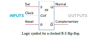
Figure 1.1: Logic symbol for a clocked R-S flip-flop
Waveform diagram for a clocked R-S flip-flop is shown in Figure 1.2.
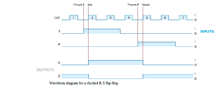
Figure 1.2: Waveform diagram for a clocked R-S flip-flop
From the diagram, it is clear that the clock pulse 1 has no effect on output Q with inputs S and R in the 0 position. The flip-flop is in the idle, or hold mode during clock pulse 1.
At the preset S position, the S (set) input is moved to 1, but output Q is not yet set to 1. Only the rising edge of clock pulse 2 permits Q to go to 1.
Pulses 3 and 4 have no effect on output Q. During pulse 3, the flip-flop is in its set mode (as S=1 and R=0), and during pulse 4, it is in its hold mode (as S=0 and R=0).
Next, input R is preset to 1. On the rising edge of clock pulse 5, the Q output is reset (or cleared) to 0. The flip-flop is in the reset mode during both clock-pulses 5 and 6 (as S=0 and R=1).
The flip-flop is in its hold mode during clock pulse7; therefore, the normal output (Q) remains at 0.
What does it mean by the synchronous operation of clocked S-R flip-flop?
From the waveform diagram for a clocked R-S flip-flop, it is clear that the outputs of the clocked R-S flip-flop change only on a clock pulse. We say that this flip-flop operates synchronously in step with the clock input. This is known as the Synchronous operation of clocked R-S flip-flop.
What does it mean by the memory characteristic of clocked S-R flip-flop?
The important characteristic of the clocked R-S flip-flop is that once it is set or reset, it stays that way even if you change some inputs. This is a memory characteristic, which is extremely valuable in many digital circuits. This characteristic is evident during the hold mode of operation. In the waveform diagram in Fig.1.2, this flip-flop is in the hold mode during clock pulses 1, 4, and 7.
Truth table for the clocked S-R flip-flop
Figure 1.3 shows a truth table for the clocked S-R flip-flop.
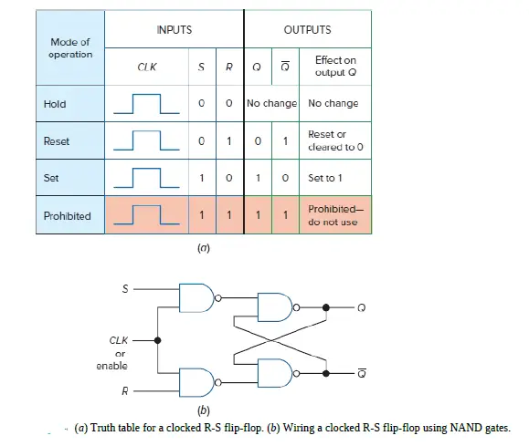
Figure 1.3 (a) Truth table for a clocked R-S flip-flop (b) Wiring a clocked R-S flip-flop using NAND gates
Notice that only the top three lines of the truth table are usable; the bottom line is prohibited and not used. Observe that the R and S inputs to the clocked R-S flip-flop are active HIGH inputs. That is, it takes a HIGH on input S while R = 0 to cause output Q to be set to 1.
Figure 1.3 shows a wiring diagram of a clocked R-S flip-flop. Notice that two NAND gates have been added to the inputs of the R-S flip-flop to add the clocked feature. The CLK input may be labeled with a C or E for enable by various manufacturers.
Clocked D Flip-Flop
The D flip-flop is often called a delay flip-flop. The word delay describes what happens to the data, or information, at input D. The data (a 0 or 1) at input D is delayed one clock pulse from getting to output Q.
The logic symbol for the D flip-flop is shown in Figure 1.4(a). It has only one data input (D) and a clock input (CLK). The outputs are labeled Q and Q’.
A simplified truth table for the D flip-flop is shown in Figure 1.4(b).
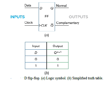
Figure 1.4 (a) Logic symbol and (b) simplified truth table for a clocked D flip-flop
From the truth table, it is clear that output Q follows input D after one clock pulse (see Qn+1 column). So in D flip-flop, Qn+1= Qn , where Qn+1 = NS (next state) and Qn =PS (present state) output of flip-flop.
Conversion of S-R flip-flop to D flip-flop
A D flip-flop may be formed from a clocked S-R flip-flop by adding an inverter between S and R and assigning the symbol D to the S input. The wiring of the D flip-flop is shown in Figure 1.5.
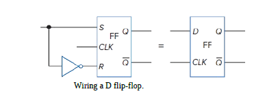
Figure 1.5 Wiring a D flip-flop from basic R-S flip-flop
The D flip-flop is either used as a delay device or as a latch to store 1 bit of binary information.
Author of this post
This post is co-authored by Professor Saraswati Saha, who is an assistant professor at RCCIIT, a renowned degree engineering college in India. Professor Saha teaches subjects related to digital electronics & microprocessors.