
Synchronous Counter Design
Last updated on June 29th, 2023 at 03:58 pm
Synchronous Counter Design – In this topic, we will now go through a step-by-step procedure to design a complete synchronous counter.
Although we will do it for a specific counting sequence (for example 00-01-10-11), the same steps can be followed for any desired sequence. This detailed guide will help the students to follow every minute step to design a Synchronous counter.
Synchronous Counter Design using JK flip flops | Synchronous Counter Design
The design steps of a 2-bit Synchronous Counter using JK flip flops are explained below in 4 steps.
Design Procedure – Step 1
Determine the desired number of bits (FFs) and the desired counting sequence.
For our example, we will design a 2-bit counter that goes through the sequence 00-01-10-11(state diagram shows the sequence of counting), so the required number of F/Fs will be 2.
Design Procedure – Step 2
Draw the state transition diagram showing all possible states, including those that are not part of the desired counting sequence.
For our example, the state transition diagram appears as shown in Figure 1, showing the desired counting sequence. The 00 through 11 states are connected in the expected sequence. We have also included a defined NEXT state (NS) for each of the PRESENT states (PS) with the excitation table of J-K flip-flop in the table given below. Here QA and QB represent the PRESENT state output whereas QA+1 and QB+1 represent the NEXT state output of FFA and FFB respectively.
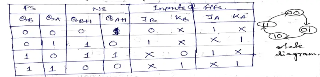
Figure 1: The state transition diagram along with the excitation table of J-K flip-flop
To understand the required flip-flop input condition for desired NEXT state the Transition table of the J-K flip-flop is very much helpful. So here is the table ( table 1) from where you can find it out very easily.
The use of the J-K transition table (Table 1) is a principal part of the synchronous counter design procedure.
Table 1: Transition table of the J-K flip-flop
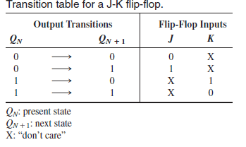
0 to 0 transition: The FF PRESENT state is at 0 and is to remain at 0 when a clock pulse is applied. From our understanding of how a J-K flip-flop works, this can happen when either J = K = 0 (no-change condition) or J = 0 and K = 1 (clear condition). Thus, J must be at 0, but K can be at either level. The table indicates this with a “0” under J and an “x” under K. Recall that “x” means the don’t-care condition.
0 to 1 transition: The PRESENT state is 0 and is to change to a 1, which can happen when either J = 1 and K = 0 (set condition) or J = K = 1 (toggle condition). Thus, J must be a 1, but K can be at either level for this transition to occur.
1 to 0 transition: The PRESENT state is 1 and is to change to a 0, which can happen when either J = 0 and K = 1 or J = K = 1. Thus, K must be a 1, but J can be at either level.
1 to 1 transition: The PRESENT state is a 1 and is to remain a 1, which can happen when either J = K = 0 or J = 1 and K = 0. Thus, K must be a 0 while J can be at either level.
From Table 2 below, you will get an idea about the transition inputs of JK flip-flops as shown in Figure 1.
Table 2: Excitation Table to find out the inputs for J-K Flip-flops
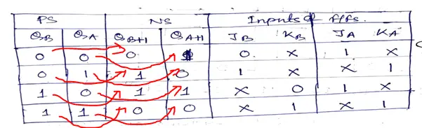
Table 2: Excitation Table to find out the inputs for J-K Flip-flops
Design Procedure Step 3
Karnaugh maps can be used to determine the logic required for the J and K inputs of each flip-flop in the counter. There is a Karnaugh map for the J input and a Karnaugh map for the K input of each flip-flop. In this design procedure, each cell in a Karnaugh map represents one of the present states in the counter sequence listed in Table 2. From the J and K states in the transition table (Table 2) a 1, 0, or X is entered into each present-state cell on the maps depending on the transition of the Q output for a particular flip-flop.
The completed Karnaugh maps for all two flip-flops in the counter are shown in Figure 2. The cells are grouped as indicated and the corresponding Boolean expressions for each group are derived.
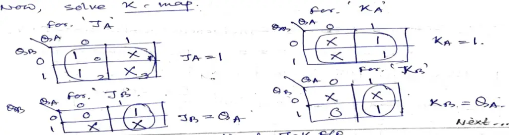
Figure2: Karnaugh maps for all the inputs of two flip-flops in the counter.
Design Procedure Step 4
Implement the counter using the J-K flip-flop to produce a specified sequence of states. Here QA is the LSB and QB is the MSB of the counter.
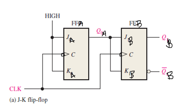
Figure 3: Logic diagram of 2-bit synchronous counter using J-K flip-flops, following the design steps mentioned above.
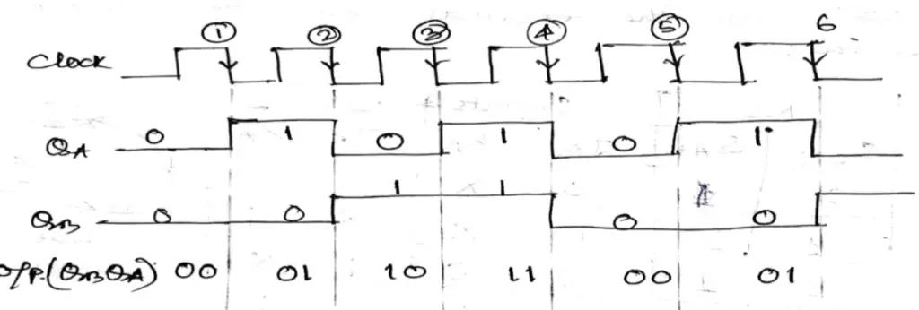
Figure 4: Timing diagram of 2-bit synchronous counter using J-K flip-flops (flip-flops are negative edge-sensitive)
Take Away
After completing this tutorial, you should be able to
- Develop a state diagram for a given sequence
- Develop a next-state table for a specified counter sequence
- Create a flip-flop transition table
- Use the Karnaugh map method to derive the logic requirements for a synchronous counter
- Implement a counter to produce a specified sequence of states
Related posts
Author of this post
This post is co-authored by Professor S. Saha, who is an assistant professor in a renowned degree engineering college in India. Professor Saha teaches subjects related to digital electronics & microprocessors.