
Memory interfacing in 8085 with RAM and ROM
Last updated on April 22nd, 2023 at 04:02 pm
In this post, we will discuss Memory interfacing in 8085 with RAM and ROM. We have covered topics like external memory support in 8085, types and sizes of memory chips, 8085 RAM and ROM size, and Pin diagrams of RAM and ROM. We have also solved interfacing problem statements using the 74LS138 decoder, and Logic gates to interface with RAM and EPROM respectively. Finally, we covered the final interfacing circuit.
- Memory interfacing in 8085 with RAM and ROM & examples
- External memory support in 8085
- Memory chips of different types and sizes | 8085 RAM and ROM size
- Pin diagram of memory chips | Pin diagram of RAM and ROM
- Interfacing RAM Chip using 74LS138 Decoder – Problem statement
- Interfacing EPROM Chip and RAM Chip using Logic Gates – Problem statement
- The final interfacing circuit
- Related Posts (8085)
Memory interfacing in 8085 with RAM and ROM & examples
In one of our previous posts, we discussed how the 8085 reads from and writes into memory. But we know that, unlike microcontrollers that have a certain amount of built-in memory, microprocessors do not have their own memory except for a few registers. So we need to attach external memory chips.
Now the question is how do we connect a memory chip to the 8085 and manage the interactions between the two chips? That is what we are going to explain in this post.
External memory support in 8085
An 8085 microprocessor has a 16-bit address bus (A0-A15). Each bit can take the value of either 0 or 1. So, the total number of addresses that can be generated on a 16-bit address bus will be 65,536. And each unique address refers to a memory block containing 8 bits or 1 byte of space.

So a maximum of 64KB (=216 Bytes) of memory locations can be interfaced with it. The memory address space of the 8085 (i.e., the range of memory addresses that can be addressed by the 8085) takes values from 0000H (A0-A15, all bits are zero) to FFFFH (A0-A15, all bits are one) when represented in hexadecimal form.
We can interface a memory chip of size less than that too. Also, we can interface several memory chips to a single 8085 microprocessor, until and unless their combined size does not exceed 64 kB.
[ Read about Foldback memory in 8085]
Memory chips of different types and sizes | 8085 RAM and ROM size
Memory chips are of different types and with different storage capacities. A broad classification of memory chips based on their read and write capability is:
- RAM (Random Access Memory): We can read as well as write data on this type of memory. The chip of this type has pins for both memory read and memory write signals.
- ROM (Read Only Memory): As the name suggests, we can only read data on this type of memory chip. The chip of this type has a pin only for memory read signal.
ROM is also of two types:
- EPROM (Erasable Programmable Read-Only Memory): The contents of an EPROM are erased by UV rays. Data is written on it optically.
- EEPROM (Electronically Erasable Programmable Read-Only Memory): As the name suggests, data is written and removed on this type of ROM electronically.
Memory chips come in different sizes like 1k X 8, 2k X 8, 4k X 8, 8k X 8, and so on. 1k means 210(=1024) locations and x 8 means each location can store 1 byte (i.e. 8 bit) of information.
So the memory size of 1k X 8 refers to 1kB memory. Similarly, 4k X 8 means 4kB memory.
Pin diagram of memory chips | Pin diagram of RAM and ROM
RAM and ROM both have the same pins, except for the WR pin, which is present in RAM and is not there in ROM. Let us understand the pins one by one.
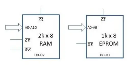
Figure1: The pins of the RAM and ROM memory chips.
- Data pins: Since each memory location stores eight bits, there are eight data lines D0-D7 connected to the memory chip.
- Address pins: The number of address pins depends on the size of the memory. In this case, a memory of size 1 kB x 8 will have 210 different memory locations. Hence, it will have ten address lines A0 to A9. Similarly, the 2 kB RAM will have 211 different memory locations. So, there are 11 address lines A0-A10.
- CS pin: When this pin is enabled, the memory chip knows that the microprocessor is communicating to it and responds to it accordingly. We need to generate this signal for each of the chips according to the range of addresses assigned to them. Basically, we select a chip only when it is needed. The Chip Select (CS) pin is used for this.
- OE pin: When this active-low output enable pin is enabled, the memory chip can output the data into the data bus.
- WR pin: Upon activation of this active-low memory write pin, data on the data bus is written on the memory chip at the location specified by the address bus.
- VCC and GND pins: These pins serve the purpose of powering the ICs. For simplicity, we will not show these pins in the diagram.
There are three types of buses in 8085 – Address bus, data bus, and control bus. Each of these buses will be connected to the memory chip.
Now, let us learn through examples, how external RAM and external ROM chips can be interfaced with 8085.
Interfacing RAM Chip using 74LS138 Decoder – Problem statement
Interface two 6116(2K X 8 RAM) ICs with the 8085 using 74LS138 Decoder such that the starting addresses assigned to them are 8000H and 9000H, respectively.
Solution:
The 6116 IC has 11 address lines (A0-A10) since 2kB=211bytes. The starting addresses assigned to 6116 chip1 and 6116 chip2 are 8000H and 9000H, respectively. So the ending addresses will be 87FFh and 97FFH respectively. Table 1 shows the binary form of the addresses 8000H to 87FFH and 9000H to 97FFH assigned to the chips.
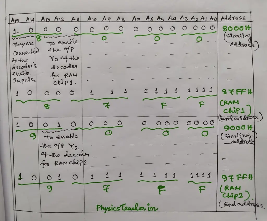
Table1: Addresses assigned to the two 6116 RAM chips (PhysicsTeacher.in)
The figure below shows the interfacing of these RAM chips with the 8085.
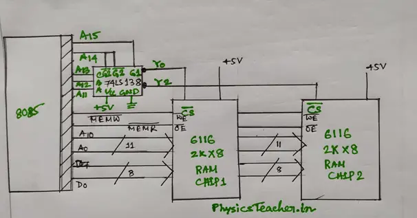
Figure2:
Interfacing two 6116 RAM chips using IC 74LS138 with the 8085. (PhysicsTeacher.in)
The address lines A0-A10 of the 8085 are connected to the address lines A0-A10 of the RAM chip.
Since the IC 74LS138 decoder has three select inputs C (MSB), B, and A (LSB), three address lines (A11, A12, and A13) of the 8085 that have a specific value for a particular RAM chip, must be connected to them. From table1 we can see that A13=A12=A11=0 for the addresses assigned to RAM chip1 and that A13=0, A12=1, and A11=0 for the addresses assigned to RAM chip2. The remaining address lines of the 8085(here A14 and A15), whose values are constant for the address ranges assigned to the two RAM chips, are connected to the enable inputs of the decoder.
Since A15=1 and A14=0 they are connected to the decoder’s active high (G1) and active low (G2A and G2B) enable inputs, respectively.
When the 8085 places any of the addresses between 8000H and 87FFH in the address bus, the select inputs C (MSB), B, and A (LSB) of the decoder are all 0.
When the 8085 places any of the addresses between 9000H and 97FFH in the address bus, the select inputs A (LSB), B, and C (MSB) of the decoder are 0,1, and 0, respectively. The Y2 output of the decoder becomes 0, selecting RAM chip2.
*MSB and LSB mean most significant, and least significant bit.
Interfacing EPROM Chip and RAM Chip using Logic Gates – Problem statement
Interface a 1kB EPROM and a 2 kB RAM with microprocessor 8085. The address allotted to 1 kB EPROM should be 3000H to 33FFH. You can assign the address range of your choice to the 2 kB RAM.
Connecting Control Signals
In the memory chips, there are two pins for control signals – OE (Output Enable) and WR (Memory Write).
While reading from a memory chip, its output should be enabled. So, MEMR will be connected to the OE pin. Similarly, for writing to a memory chip, MEMW will be connected to the WR pin of the RAM. After completing these two connections, we need to enable the CS line.
Data Bus interfacing
There are eight lines comprising the data bus of both 8085 and the memory chips. The interfacing of the data bus is the simplest part. We just connect the corresponding lines (D0-D7 from 8085) to the corresponding pins (D0-D7 of the memory chip).
Address bus Interfacing
We have a 2kB RAM with 11 address lines. So, the first 11 lines of the address bus of 8085 will be connected to the corresponding address lines of the 2kB RAM. Similarly, the first 10 lines of the address bus of 8085 will be connected to the corresponding lines of 1kB EPROM. The remaining address lines will be used to generate the chip select (CS) signal.
Generating the chip select signal
This is a little tricky, but it’s the most important part of solving the problem. Let us proceed step by step and build up an intuition of how to generate the chip select signal for a memory of a given size and given address range.
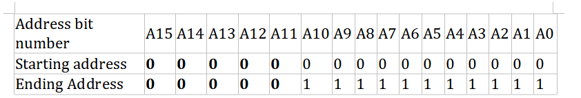
Let us tabulate the starting and ending address of the 1kB EPROM.
A15 is the most significant, and A0 is the least significant bit. The address range for placing the EPROM is from 3000H to 33FFH (as given in the question.) Translating these to binary:
3000H = 0011 0000 0000 0000
33FFH = 0011 0011 1111 1111
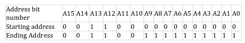
From the above table, we can observe that ten bits from A0 to A9 are changing. These ten bits are directly connected to the address lines of the memory chip.
These ten bits take the value of either 0 or 1 to form addresses. The first address is 00 0000 0000, the second address is 00 0000 0001, the third is 00 0000 0010, and so on. The last address will be 11 1111 1111.
Meanwhile, bits A10 to A15 do not change and don’t have any effect on the addressing process inside the memory chip. So, we can conclude that the values of bits A15-A10 (0011 00) given in the above table are in a unique, unchanging configuration for this memory chip. If even one of these bits changes, the address won’t belong to this memory chip. So, we can use these values of A15-A10 to uniquely identify this memory chip, which is exactly what the CS signal is supposed to do.
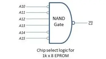
We can say that when A15 = A14 =A11 = A10 = 0 and A13=A12 = 1, then our memory chip should be selected. Now, we need to design the logic to generate the CS signal.
The resulting Boolean equation of CS will be:
CS = Complement of (A15*. A14*. A13 . A12 . A11* . A10*)
This equation can be implemented using NAND Gate. The final chip select logic for 1kB EPROM is illustrated below.
Now, we have to generate a chip select signal for the second memory chip, which is 2kB RAM. The process is quite similar and differs from the previous one in two ways:
- The size of the memory is different. So, there are 11 address lines instead of 10.
- We are not given an address range here. We are given the liberty to decide on our own.
Similar to the previous case, we connect the first 11 address lines of the 8085 microprocessor to the 11 address lines of the 2kB RAM. These bits will take values of 0 and 1 and will generate 2 * 1024 different addresses. The address bits A10-A0 will vary from 000 0000 0000 to 111 1111 1111.
What about the remaining address bits? Well, they don’t have any role in the addressing of the memory in this 2kB RAM. So, we can fix them to a certain value without affecting anything. Let’s fix them to 0000 0. Thus, the address range for this chip becomes 0000 0000 0000 0000 to 0000 0111 1111 1111. In hexadecimal, the address range will be from 0000H to 07FFH.
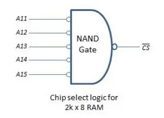
We use a similar technique here. We use the remaining bits A15-A11 to uniquely identify this chip i.e., to generate the chip select signal. So, the Boolean equation will be
CS = Complement of (A15* . A14* . A13* . A12* . A11*)
The implementation of this equation using the NAND Gate to generate the CS signal is shown in the following image.
The final interfacing circuit
Since we have the chip select logic and have decided on all the connections, it’s time to finalize the circuit. The entire external memory interfacing circuit can be broken up into five different parts:
- 8085 microprocessor
- De-multiplexing of address/data bus using 74LS373Latch
- Generation of control signals using 74LS138 Decoder
- Generation of chip select signals using NAND gates
- Memory chips
The image below shows the final circuit with all the five parts listed above integrated into a single circuit.
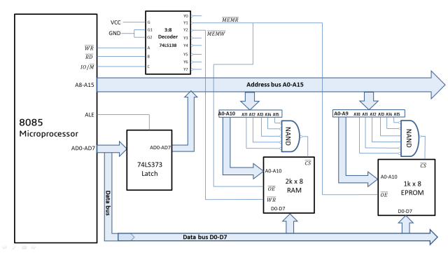
Figure3:
External memory interfacing circuit with 8085 microprocessor – Block diagram
The above block diagram summarizes the entire process of interfacing the external memory with the 8085 microprocessor.
Author of this post
This post is co-authored by Professor Saraswati Saha, who is an assistant professor at RCCIIT, a renowned degree engineering college in India. Professor Saha teaches subjects related to digital electronics & microprocessors.
Related Posts (8085)
8085 Interrupts with pdf download
8085 – methods of Data Transfer
MCQs on 8085 Instruction set, Addressing Modes & Machine cycles
How to Interface a RAM chip with 8085 microprocessor
Functional block diagram of Intel 8085 microprocessor and the functional units
General purpose registers of 8085 microprocessor
Special-purpose registers of 8085 microprocessor – FAQs
Architecture of 8085 microprocessor
Instruction Word flow diagram and Data Word flow diagram for Intel 8085 & 8086
Fetch Cycle, Instruction Cycle, Machine Cycle & T-state of 8085 & 8086 Microprocessor – FAQs
De-Multiplexing of AD0-AD7 in 8085 Microprocessor
Instruction Set and Types of instruction in 8085 microprocessor – FAQs
FAQs on addressing modes of instructions | execution of an instruction in 8085 microprocessor
Arithmetic Instructions in 8085 Microprocessor for Arithmetic operations: Revision notes
8085 Microprocessor – tutorials (hub)
Microprocessor class notes – PDF download