
Demultiplexing of address and data bus in 8085
Last updated on August 4th, 2022 at 08:29 pm
In this post, we will see how Demultiplexing of multiplexed address and data bus AD7-AD0 in 8085 is done. The 8085 uses a multiplexed data bus and address bus. This means the Lower address bus (A7 – A0) and the data bus (D7 – D0) are available on the same pins AD7 – AD0.
Multiplexing is done to reduce the number of pins of 8085. However, external memory or I/O devices need the separate 16-bit address A15 – A0 for decoding and selecting a device and separate D7 – D0 for data transfer.
So, the multiplexed address-data bus must be demultiplexed so that the memory and I/O devices will have a separate address bus A15 – A0 and data bus D7 – D0. The demultiplexing can be done with the help of the ALE signal (Address Latch Enable) given out by the processor for this purpose.
Demultiplexing of address and data bus in 8085 with ALE signal
Pin 30 of 8085 is the ALE pin which stands for ‘Address Latch Enable’. ALE signal is used to demultiplex the lower order address bus (AD0 – AD7).
Pins 12 to 19 of 8085 are AD0 – AD7 which represents the multiplexed address-data bus.
Multiplexing is done to reduce the number of pins of 8085. The lower byte of address (A0 – A7) is available from AD0 – AD7 (pins 12 to 19) during the T1 of the machine cycle. But the lower byte of address (A0 – A7), along with the upper byte
A8 – A15 (pins 21 to 28) must be available during T2 and the rest of the machine cycle to access memory location or I/O ports.
Now ALE signal goes high at the beginning of T1 of each machine cycle and goes low at the end of T1 and remains low during the rest of the machine cycle.
This high to low transition of ALE signal at the end of T1 is used to latch the lower order address byte (A0 – A7) by the latch IC 74LS373 so that the lower byte A0 – A7 is continued to be available till the end of the machine cycle.
The situation is explained in the following figure:
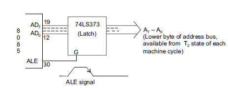
The Lower byte of address latching is achieved by the H to L transition of the ALE signal, which occurs at the end of T1 of each machine cycle.
Why the lower-byte address bus (A0 – A7) and data bus (D0 – D7) are multiplexed?
This is done to reduce the number of pins of 8085, which otherwise would have been a 48 pin chip. But because of multiplexing, external hardware is required to de-multiplex the lower order multiplexed address-data bus.
Author of this post
This post is co-authored by Professor Saraswati Saha, who is an assistant professor at RCCIIT, a renowned degree engineering college in India. Professor Saha teaches subjects related to digital electronics & microprocessors.
Related Posts
8085 Interrupts with pdf download
8085 – methods of Data Transfer
MCQs on 8085 Instruction set, Addressing Modes & Machine cycles
How to Interface a RAM chip with 8085 microprocessor
Functional block diagram of Intel 8085 microprocessor and the functional units
General purpose registers of 8085 microprocessor
Special-purpose registers of 8085 microprocessor – FAQs
Architecture of 8085 microprocessor
Instruction Word flow diagram and Data Word flow diagram for Intel 8085 & 8086
Fetch Cycle, Instruction Cycle, Machine Cycle & T-state of 8085 & 8086 Microprocessor – FAQs
De-Multiplexing of AD0-AD7 in 8085 Microprocessor
Instruction Set and Types of instruction in 8085 microprocessor – FAQs
FAQs on addressing modes of instructions | execution of an instruction in 8085 microprocessor
Arithmetic Instructions in 8085 Microprocessor for Arithmetic operations: Revision notes
8085 Microprocessor – tutorials (hub)
Microprocessor class notes – PDF download