
How to Interface a RAM chip with 8085 microprocessor
Last updated on March 5th, 2022 at 05:12 am
In this post, we have discussed the interfacing of a 1 KB RAM chip with the 8085 microprocessor. We have also discussed the Memory mapping of the RAM chip. Steps followed by the 8085 microprocessor to read the content of a memory location in the RAM chip are also discussed.
We know that the programs and data that are executed by the microprocessor have to be stored in ROM/EPROM and RAM, which are basically semiconductor memory chips.
Since the 8085 microprocessor has 16-bit wide address lines (A0-A15), a maximum of 64KB (=216 Bytes) of memory locations can be interfaced with it.
The memory address space of the 8085 (i.e., the range of memory addresses that can be addressed by the 8085) takes values from 0000H (A0-A15, all bits are zero) to FFFFH (A0-A15, all bits are one) when represented in hexadecimal form.
While executing a program, the 8085 microprocessor needs to access the memory regularly to read instructions and data and to store results.
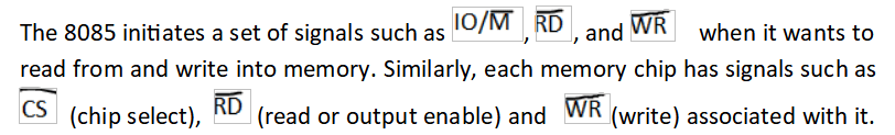
The memory interfacing circuit must match the processor’s signals to the memory chip’s signals.
Table 1 shows the relation between the 8085’s control signals and the memory chip’s control signals.
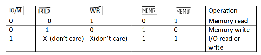
Table 1: Relation between the 8085’s control signals and the memory chip’s control signals.
While the 8085 has 16 address lines, the number of address lines in a memory chip depends on the storage capacity of the chip.
For example, an 1K Byte (1024X8) RAM chip has only 10 address lines (since 210 bytes=1KB).
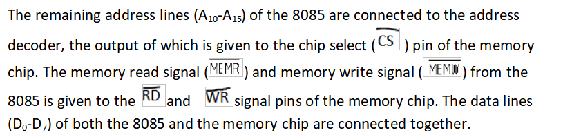
The lower-order address lines (A0-A9) of the 8085 are connected to the address lines (A0-A9) of the 1 KByte Memory chip.
Interfacing a 1KB (1K X 8) RAM chip with 8085 Microprocessor and the address ranges assigned to the RAM chip
We know that in a 1KB (1K X 8) RAM chip, there are 1024 memory locations and each location can store one byte(i.e. 8 bit)of information(instructions or data).
There are 10 address lines (since 210 bytes=1KB) A0-A9 in the IC chip, where A0 is the least significant bit of the address and A9 is the most significant bit. They are used to select memory locations in the IC during the memory read and write operation.
Interfacing of a 1KB (1K X 8) RAM chip with an 8085 Microprocessor is explained with the help of figure 1 given below.
Also, the address ranges assigned to the RAM chip are discussed with the help of table 2.
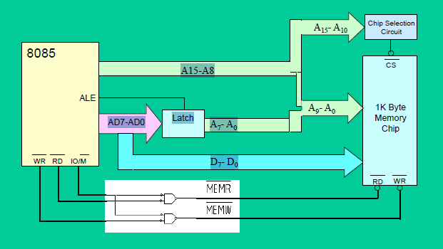
Figure 1: Interfacing 1KB RAM chip with 8085 Microprocessor
The address assigned to the RAM chip or Address map (the set of addresses assigned to the memory chip in a system is called a memory address map)is shown in the table below. Since the IC has 10 address lines, a partition is made between A0-A9 and the remaining address lines A10-A15.
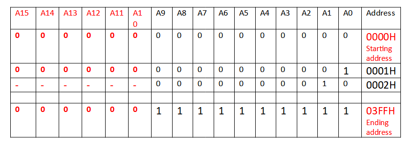
Table2: Address assigned to 1KB RAM chip – Address map
The starting address assigned to this chip is 0000H. To find the ending address, add the hexadecimal value of a 10–bit binary number with all bits equal to 1 (3FFH) to the starting address of the chip.
10 – bit binary number with all bits equal to 1————–11 1111 1111
corresponding hexadecimal number————————-3 F F
The ending address of the chip is 0000H + 03FFH= 03FFH
Steps followed by the 8085 microprocessor to read the content of a memory location in the RAM chip
Step1: The address of memory location from where data has to be read is placed in the address lines of the RAM.
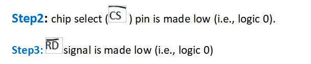
After this, the data in the selected memory location is available in the data lines (D0-D7) of the RAM. The 8085 microprocessor reads the data in the data lines.
Author of this post
This post is co-authored by Professor Saraswati Saha, who is an assistant professor at RCCIIT, a renowned degree engineering college in India. Professor Saha teaches subjects related to digital electronics & microprocessors.
Related Posts
8085 Interrupts with pdf download
8085 – methods of Data Transfer
MCQs on 8085 Instruction set, Addressing Modes & Machine cycles
How to Interface a RAM chip with 8085 microprocessor
Functional block diagram of Intel 8085 microprocessor and the functional units
General purpose registers of 8085 microprocessor
Special-purpose registers of 8085 microprocessor – FAQs
Architecture of 8085 microprocessor
Instruction Word flow diagram and Data Word flow diagram for Intel 8085 & 8086
Fetch Cycle, Instruction Cycle, Machine Cycle & T-state of 8085 & 8086 Microprocessor – FAQs
De-Multiplexing of AD0-AD7 in 8085 Microprocessor
Instruction Set and Types of instruction in 8085 microprocessor – FAQs
FAQs on addressing modes of instructions | execution of an instruction in 8085 microprocessor
Arithmetic Instructions in 8085 Microprocessor for Arithmetic operations: Revision notes
8085 Microprocessor – tutorials (hub)
Microprocessor class notes – PDF download