
Instruction Word flow diagram and Data Word flow diagram for Intel 8085 & 8086
Last updated on March 10th, 2022 at 05:32 pm
In this post, we will draw the Instruction Word flow diagram and Data Word flow diagram for general-purpose microprocessors like Intel 8085 and 8086 and then explain the sequence of operations related to these diagrams.
Draw the block schematic of a typical Instruction Word flow diagram and explain the same
The Instruction Word flow diagram (flow diagram for instruction word) is shown below (figure 1).
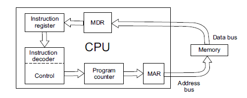
Figure 1: Flow of instruction word
The sequence of operation of the instruction word flow for general-purpose microprocessors is explained below:
The 2 byte content of the PC (program counter) is transferred to a special register–called memory address register (MAR) or simply address register (AR) at the beginning of the fetch cycle.
Since the content of MAR is an address, it is thus sent to memory via the address bus.
The content of the addressed memory is then read under the ‘Read control’ generated by the T&C (Timing and control unit) section of the microprocessor.
This is then sent via the data bus to the memory data register (MDR) or the data register (DR) existing in the CPU. This is placed in the instruction register
(IR) and is decoded by the instruction decoder and subsequently executed.
The PC is then incremented if the subsequent memory location is to be accessed.
Draw the block schematic of a typical Data Word flow diagram and explain the same
The data word flows via the data bus into the accumulator.
The block schematic of the data word flow diagram is shown below (figure 2).
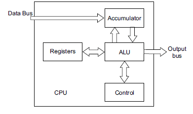
Figure 2: Flow of data word
The sequence of operation of the data word flow is explained below:
The data source can be a memory device or an input device. Data will be loaded into the accumulator via input Data Bus (DB).
Data from the accumulator is then manipulated in ALU (Arithmetic and logic unit) under the control of the T & C (Timing and control) unit.
The manipulated data is then put back in the accumulator and can be sent to memory or output devices through the output Data Bus.
Author of this post
This post is co-authored by Professor Saraswati Saha, who is an assistant professor at RCCIIT, a renowned degree engineering college in India. Professor Saha teaches subjects related to digital electronics & microprocessors.
Related Posts
8085 Interrupts with pdf download
8085 – methods of Data Transfer
MCQs on 8085 Instruction set, Addressing Modes & Machine cycles
How to Interface a RAM chip with 8085 microprocessor
Functional block diagram of Intel 8085 microprocessor and the functional units
General purpose registers of 8085 microprocessor
Special-purpose registers of 8085 microprocessor – FAQs
Architecture of 8085 microprocessor
Instruction Word flow diagram and Data Word flow diagram for Intel 8085 & 8086
Fetch Cycle, Instruction Cycle, Machine Cycle & T-state of 8085 & 8086 Microprocessor – FAQs
De-Multiplexing of AD0-AD7 in 8085 Microprocessor
Instruction Set and Types of instruction in 8085 microprocessor – FAQs
FAQs on addressing modes of instructions | execution of an instruction in 8085 microprocessor
Arithmetic Instructions in 8085 Microprocessor for Arithmetic operations: Revision notes
8085 Microprocessor – tutorials (hub)
Microprocessor class notes – PDF download