
Interfacing of 8255 PPI with 8085 microprocessor
Last updated on May 18th, 2022 at 05:28 pm
PPI 8255 is a general-purpose programmable I/O device designed to interface the CPU with its outside world such as ADC, DAC, keyboard, etc. We can program it according to the given condition. It can be used with almost any microprocessor. Here in this post, we will discuss the interfacing of 8255 PPI with 8085 microprocessor in I/O mode & BSR mode through various examples.
Every programmable device will have one or more CONTROL-REGISTERS. It can be set up to perform specific functions by writing CONTROL-WORDS into the control register. The control-word format is specified by the manufacturer of the peripheral device.
8255 PPI has three programmable ports and one control register.
- Control word in 8255 PPI
- Operational Modes of 8255A
- Chip-select logic for 8255 in 8085 microprocessor-based system
- Different ports and control register selection for 8255
- BSR mode and its characteristics
- Control word format in the BSR mode
- Programming in BSR mode
- Control word format for I/O mode operation of PPI 8255
Control word in 8255 PPI
The content of the control register is called the control word (8 bit wide), specifying an I/O function for each port. Bit D7 of the control register specifies either the I/O function or the Bit Set/Reset (BSR) function.
Operational Modes of 8255A
The operational mode of 8255A PPI can be classified into two broad groups.
1) Input-Output mode (I/O mode)
2) Bit set reset mode (BSR mode)
The I/O mode is further classified into three modes: Mode 0, Mode 1, and Mode 2, as shown in the figure below.
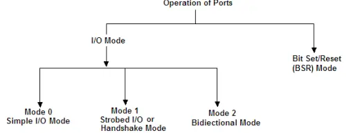
Fig.1 Operational Modes of 8255A
Input-Output mode
If MSB of control word (D7) is 1, PPI works in input-output mode. This is further divided into three modes:
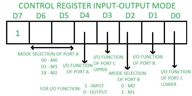
Fig.2 Control register of 8255 PPI in I/O mode
- Mode 0 – In this mode, all the three ports (ports A, B, and C) can be programmed to function as simply an input port or an output port. In this mode, there is no interrupt handling capacity.
- Mode 1 – Handshake I/O mode or strobed I/O mode. In this mode, either port A or port B can work as a simple input port or simple output port, and port C bits are used for handshake signals before actual data transmission. It has interrupt handling capacity and input and output data are latched.
- Mode 2 – Bi-directional data transfer mode. In this mode only port A works, and port B can work either in mode 0 or mode 1. Port-A uses five signals from port C as handshake signals for data transfer. The remaining three signals from port C can be used either as simple I/O or as a handshake for port- B. It also has interrupt handling capacity.
Bit set reset (BSR) mode
If the MSB of the control word (D7) is 0, PPI works in BSR mode. In this mode, only port C bits are used for the set or reset.
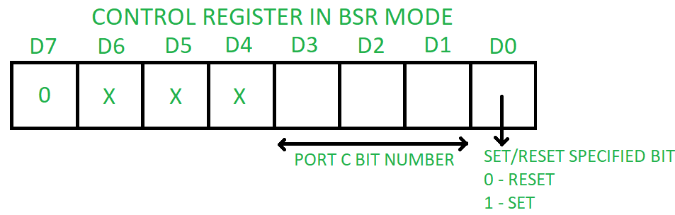
Fig.3 Control register of 8255 PPI in BSR mode
Chip-select logic for 8255 in 8085 microprocessor-based system
Generally, the microprocessor kits available with the laboratories have two 8255 connected with the system; 8255-I and 8255-II.
Fig. 4 shows the chip-select logic for 8255-I. From this logic diagram, it is clear that if AD7-AD2 pins are all 0s then it enables CS (Active low) to select this chip.
The port selection will depend on the bits AD1-AD0 as given in table 1.
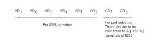
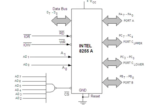
Fig. 4 chip-select logic for 8255-I
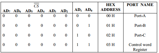
Fig.5 shows the chip select logic for the 8255-II. If AD7-AD2 pins are chosen as per this diagram then the second 8255 (8255-II) will be selected.
The port selection will depend on the bits AD1-AD0 as given in table2.
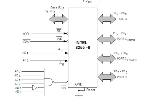
Fig.5 Chip select logic for 8255-II
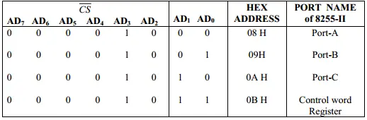
Table2. The port selection will depend on the bits AD1-AD0
It may be mentioned here that if the instruction OUT 03 H is executed then it transfers the contents of the accumulator to the control word register of 8255-I. Similarly, if the instruction OUT OB H is executed then the accumulator contents will be transferred to the control word register of 8255-II.
For the control word, the accumulator is loaded with the contents that are necessary to use the ports of 8255 as an input port or output port. The procedure for the generation of control word will be discussed now.
Now if 8255-I is initialized to use Port A as input port and ports B and C as output ports, then the execution of IN 00 H (00H is the address of Port A) instruction will transfer the data from port A of 8255-I to the accumulator. The execution of OUT 01 H (01H is the address of Port-B) instruction will transfer the accumulator contents to port B of 8255-I.
Similarly, 8255-II may be initialized by giving the proper control word to the control word register by using the instruction OUT 0B H. The IN or OUT instruction having the port address as 08, 09, or 0A may be used for the data transfer through 8255-II.
Different ports and control register selection for 8255
The two address lines, along with the CS signal, determine the selection of a particular port or control register. This is explained below:
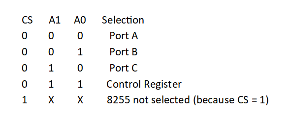
CS signal is made 0 by choosing A7 = 1 and A6 through A2 = 0.
BSR mode and its characteristics
BSR mode stands for Bit Set Reset mode.
The characteristics of BSR mode are:
1) BSR mode is selected only when D7 = 0 of the Control Word Register (CWR).
2) Concerned with bits of port C.
3) Individual bits of Port C can either be Set or Reset.
4) At a time, only a single bit of port C can be Set or Reset.
5) It is used for control or on/off switch.
6)BSR control word doesn’t affect ports A and B functioning.
Control word format in the BSR mode
The content of the control word register will be as follows, when used in the BSR mode and selects (either Sets or Resets) a particular bit of Port C at a time.
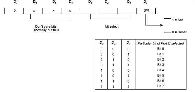
Programming in BSR mode
Example: Write a BSR control word to set bits PC7 and PC0 and reset them after a 1-second delay.
Solution: To set or reset any particular bit of Port C in the BSR mode, the control word register is to be appropriately loaded. The above is done by loading the accumulator and sending the same to the control register (i.e., by sending the same to the address of the control register).
Consider that the address of the control word register (CWR) is 83H.
Program:
MVIA, 0FH (Accumulator loaded with 0FH to set PC7 bit of Port C)
OUT 83H (This sets PC7 bit of Port C)
MVIA, 01H (Accumulator loaded with 01H to set PC0 bit of Port C)
OUT 83H (This sets PC0 bit of Port C)
CALL DELAY (Assume the DELAY is for 1 second)
MVIA, 00H (Accumulator loaded with 00H to reset PC0 bit of Port C)
OUT 83H (This resets PC0 bit of Port C)
MVIA, 0EH (Accumulator loaded with 0EH to reset PC7 bit of Port C)
OUT 83H (This resets PC7 bit of Port C)
Control word format for I/O mode operation of PPI 8255
The control word format, when 8255 is operated in I/O mode, is shown below:
For 8255 PPI to be operated in I/O mode, the D7 bit must be 1.
The three ports are clubbed into two groups—Groups A and B.
Group A consists of Port A and Port C upper. Port A can be operated in any of the modes—0, 1, or 2.
Group B consists of Port B and Port C lower. Here Port B can be operated in either mode 0 or 1.
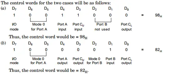
Example: Write down the mode 0 control words for the following two cases:
(a) Port A = Input port, Port B = not used, Port CU = Input port and Port CL = Output port.
(b) Port A = Output port, Port B = Input port, Port C = Output port
Solution
Author of this post
This post is co-authored by Professor Saraswati Saha, who is an assistant professor at RCCIIT, a renowned degree engineering college in India. Professor Saha teaches subjects related to digital electronics & microprocessors.