
Memory organization in 8086 microprocessor
Last updated on May 9th, 2022 at 01:07 pm
After studying this article the readers will be able to understand the physical memory organization, 20-bit address generation technique, the need for memory segmentation, etc. in 8086 microprocessor. Frequently asked questions (FAQs) and their detailed answers in this post are going to help the readers to prepare for the Semester exam, GATE exam, and the technical interview.
- Logical address, base segment address, and physical address in the 8086 microprocessor
- 20-bit physical address generation in the 8086 microprocessor
- Which pins identify the segment registers used for 20-bit physical address generation in the 8086 microprocessor?
- Although 8086 is a 16-bit microprocessor, it deals with 8-bit memory. Why?
- What is the maximum size of the memory that can be accessed by 8086?
- Mention the address capability of 8086 and also show its memory map.
- Memory organization in 8086 microprocessor | How memory is organized in the 8086 Microprocessor?
- What is the maximum size of the memory that can be accessed by 8086?
- Explain the concepts of even and odd memory banks in 8086.
- Define the term memory segmentation in a computer system.
- Mention the different types of memory segmentation of 8086.
- Describe the memory segmentation scheme of 8086.
- Why memory segmentation is done for 8086?
- What are the rules of segmentation in 8086 microprocessors?
- Mention the names of segment registers and the default offset registers in the 8086.
Logical address, base segment address, and physical address in the 8086 microprocessor
The logical address also termed an effective address or offset address, is contained in the 16-bit IP, BP, SP, BX, SI, or DI. The 16-bit content of one of the four-segment registers (CS, DS, ES, SS) is known as the base segment address.
Offset and base segment addresses are combined to form a 20-bit physical address (also called a real address) that is used to access the memory. This 20-bit physical address is put on the address bus (AD19 – AD0) by the BIU (Bus interface unit) in the 8086 microprocessor.
20-bit physical address generation in the 8086 microprocessor
The 20-bit physical (real) address is generated by combining the offset (residing in IP, BP, SP, BX, SI, or DI) and the content of one of the segment registers CS, DS, ES, or SS.
The process of combination is as follows:
The content of the segment register is internally appended with 0 H (0000 H) on its rightmost end to form a 20-bit memory address—this 20-bit address points to the start of the segment. The offset is then added to the above to get the physical address.
Fig. 1 shows pictorially the actual process of generating a 20-bit physical address.
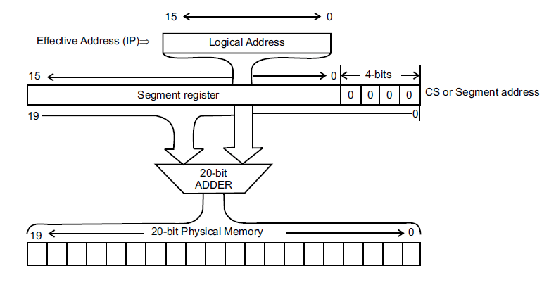
Fig.1: 20-bit Physical address generation in 8086 microprocessor.
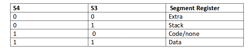
Which pins identify the segment registers used for 20-bit physical address generation in the 8086 microprocessor?
Pins A16 and A17 become S3 and S4 from the second bus cycle. This 2-bit combination of S3 and S4 indicates the segment register used for physical address generation and is shown in Table. The two status lines are output both in the maximum and minimum mode.
Table 1 identifies the segment register used for 20-bit physical address generation.
Although 8086 is a 16-bit microprocessor, it deals with 8-bit memory. Why?
This is so for the following two reasons:
- It enables the microprocessor to work with both bytes and words. This is very important because many I/O devices such as printers, terminals, modems, etc, transfer ASCII coded data (7 or 8 bits).
- Quite a few of the operation codes of 8086 are single bytes while so many other instructions are there which vary from 2 to 7 bytes. By working with byte-width memory, these varied operation codes can easily be handled.
What is the maximum size of the memory that can be accessed by 8086?
8086, via its 20-bit address bus, can address 220 = 1,048,576 or 1 MB of different memory locations. Thus the memory space of 8086 can be thought of as consisting of 1,048,576 bytes or 524,288 words (1 word= 2 bytes).
Mention the address capability of 8086 and also show its memory map.
The memory map of 8086 is shown in Fig. 2, where the whole memory space
starting from 00000 H to FFFFF H is divided into 16 blocks-each one consisting of 64 KB.
This division is arbitrary but at the same time, a convenient one because the most significant hex digit increases by 1 with each additional block. Thus, the 30000 H memory location is 65,536 bytes higher in memory than the memory location 20000 H.
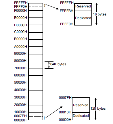
Fig. 2: The memory map of 8086
The lower and upper ends of the memory map are shown separately-marking some spaces as reserved and some as ‘dedicated’. The reserved locations are meant for future hardware and software needs while the dedicated locations are used for processing of specific system interrupts and reset functions.
Memory organization in 8086 microprocessor | How memory is organized in the 8086 Microprocessor?
The total address space of 1 MB of 8086 is divided into 2 banks of memory – each bank of a maximum size of 512 KB. One is called the high order memory bank (or high bank) and the other low order memory bank (or low bank).
Low bank, high bank, or both banks can be accessed by utilizing two signals BHE (Bus high enable) and A0 (LSB of address bus). Both are active low.
Table 2 shows the three possible references to memory.
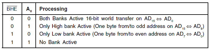
The high bank is selected for A0=1 and BHE=0 and is connected to D15–D8 while the low bank is selected for A0=0 and BHE =1. Neither the low bank nor the high bank would be selected for A0=1 and BHE =1.
Fig. 3 shows how the total address space (1MB) of 8086 is physically implemented
by segregating it into low and high banks. It also shows that the CS signal of the high bank is connected to BHE while the CS signal of the low bank is connected to A0.
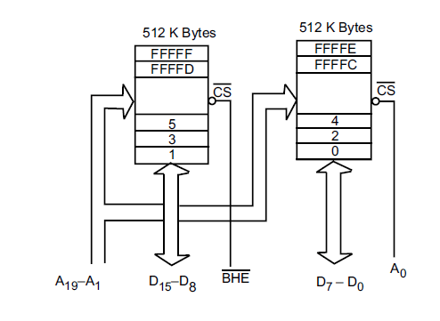
Fig. 3: Physical implementation of 1MB memory in 8086 microprocessor by
segregating it into low (Even) and high (odd) banks.
What is the maximum size of the memory that can be accessed by 8086?
The two status codes S4 and S3 together point to the segment register used for 20-bit physical address generation and can be examined by external circuitry to enable separate 1 MB address space for each of CS, ES, DS, and SS. This would enable the memory address to be expanded to a maximum of 4MB for 8086 μP.
Explain the concepts of even and odd memory banks in 8086.
The low and high-order memory banks correspond to even and odd banks respectively. The CS (Chip select) signal of low order memory bank is selected when CS = 0. Since A0 (lowest address bus line) is connected to CS, hence A0 must be low for the low order bank to be selected. That is why the low-order bank corresponds to the even bank. Similarly, the high order bank is selected when A0 = 1. Hence, the higher-order bank is called the odd bank.
The profile of the low and high order banks are shown below in Fig. 4
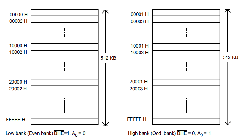
Fig. 4: The profile of the low and high-order banks in 8086.
Define the term memory segmentation in a computer system.
Segmentation is the process in which the main memory of the computer is logically divided into different segments and each segment has its own base address. It is basically used to enhance the speed of execution of the computer system so that the processor is able to fetch and execute the data from the memory easily and fast.
Mention the different types of memory segmentation of 8086.
The different memory segmentation in the case of 8086 includes
- Continuous
- Partially overlapped
- Fully overlapped and
- Disjointed
This is shown in Fig.5
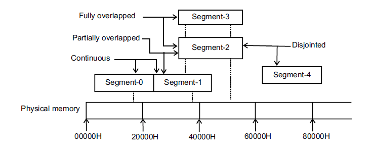
Fig. 5: Depiction of different types of segments
In the figure,
Segments-0 and 1 ——– Continuous
Segments-1 and 2 ———Partially overlapped
Segments-2 and 3 ———Fully overlapped
Segments-2 and 4 ———Disjointed
Describe the memory segmentation scheme of 8086.
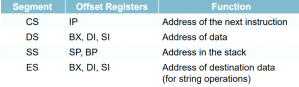
1 MB memory of 8086 is partitioned into 16 segments – each segment is 64 KB in length. Out of these 16 segments, only 4 segments can be active at any given instant of time—these are the code segment, stack segment, data segment, and the extra segment.
The four memory segments that the CPU works with at any time are called currently active segments. Corresponding to these four segments, the registers
used are Code Segment Register (CS), Data Segment Register (DS), Stack Segment Register (SS), and Extra Segment Register (ES) respectively.
Each of these four registers is 16-bits wide and user-accessible—i.e., their contents can be changed by software.
The code segment contains the instruction codes of a program, while data, variables, and constants are held in the data segment. The stack segment is used to store interrupt and subroutine return addresses. The extra segment contains the destination of data for certain string instructions.
Thus 64 KB are available for program storage (in CS) as well as for stack (in SS) while 128 KB of space can be utilized for data storage (in DS and ES).
One restriction on the base address (starting address) of a segment is that it must reside on a 16-byte address memory—examples being 00000 H, 00010 H, or 00020 H, etc.
Why memory segmentation is done for 8086?
Memory segmentation, as implemented for 8086, gives rise to the following advantages:
- Although the address bus is 20-bits in width, memory segmentation allows one to work with registers having a width of 16-bits only.
- It allows instruction code, data, stack, and the portion of the program to be more than 64 KB long by using more than one code, data, extra segment, and stack segment.
- In a time-shared multitasking environment when the program moves over from one user’s program to another, the CPU will simply have to reload the four-segment registers with the segment starting addresses assigned to the current user’s program.
- The user’s program (code) and data can be stored separately.
- Because the logical address range is from 0000 H to FFFF H, the same can be loaded at any place in the memory.
What are the rules of segmentation in 8086 microprocessors?
The segmentation process follows some rules as follows:
- The starting address of a segment should be such that it can be evenly divided by 16.
- The minimum size of a segment can be 16 bytes and the maximum can be 64 kB.
Mention the names of segment registers and the default offset registers in the 8086.
The segment registers and the default offset registers in the 8086 are explained with the help of the table given below.
Author of this post
This post is co-authored by Professor Saraswati Saha, who is an assistant professor at RCCIIT, a renowned degree engineering college in India. Professor Saha teaches subjects related to digital electronics & microprocessors.