
Foldback Memory in 8085 microprocessor with example
Last updated on April 22nd, 2023 at 05:15 pm
In this post, we will discuss the concepts of Foldback Memory in 8085 microprocessor with an example. To understand that, we will first discuss about the address decoding technique to select a particular memory chip in a 8085 microprocessor-based system, and the memory addresses for the selected chip. Then we will study the concepts of foldback memory with an example.
What is foldback memory? | What is foldback memory in 8085 microprocessor?
Address lines of microprocessors that are not used for selecting the memory chip and remain in the don’t care condition create different sets of memory ranges along with the primary range. These set of memory ranges are known as either foldback memory or mirror memory.
Address decoding and Memory Addresses
In any 8085 microprocessor-based system, the processor should be able to read data from the memory and write data into the memory. To fulfill this purpose proper interfacing circuit is required between the microprocessor and the memory chip. [ Learn more about Memory interfacing with RAM and ROM]
Address decoding with Example
Figure 1 shows an interfacing circuit using a 3-to-8-line decoder to interface the 6116 memory chip with 2048(2k) registers. The memory chip requires 11 (211=2048) address lines (A10-A0) to decode 2048 registers.
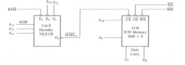
Figure 1: Interfacing circuit between the microprocessor and 6116 memory chip.
From the figure, it is clear that the 8085 address lines A10-A0 are connected to pins A10-A0 of the memory chip to decode 2048 registers. The remaining address lines A15-A11 are connected to the decoder.
However, in this circuit, the decoder is enabled by the IO/M’ signal in addition to the address lines A15 and A14, and the RD’ and WR’ signals of the 8085 are directly connected to the memory chip.
The output line O1 of the decoder is connected to CE’ of the memory chip, and it is identified as MSEL1 (Memory select) because it is asserted only when IO/M’ is low.
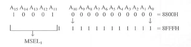
Therefore the memory address of this chip ranges from 8800H to 8FFFH, as shown above. Now to examine how an address is decoded and how the microprocessor reads from this memory, let us assume that the 8085 places the address 8FFFH on the address bus.
The 10001 (from the left side) goes to the decoder, the decoder becomes enabled and the O1 of the decoder selects chip 6116. The remaining address bits( 111 1111 1111) go on the address lines of the chip, and the internal decoder of the memory chip decodes the address and selects the register.
Interfacing between processor and memory chip
When the 8085 microprocessor asserts the RD’ signal, the output buffer is enabled and the contents of the register are placed on the data bus for the processor to read.
When the 8085 microprocessor asserts the WR’ signal, the input buffer is enabled and the contents over the data bus are placed into the register for the processor to write.
Foldback Memory with example
Figure 2 shows the interfacing circuit between the 8085 microprocessor and the 8115 memory chip. From the figure, it is clear that the 8085 multiplexed address data lines AD7-AD0 are connected to pins A7-A0 of the memory chip to decode 256 registers.
The address lines A15-A11 are connected to the decoder. However, in this circuit, the decoder is enabled when A15 and A14 are 00.
The address lines A13-A11 are connected as an input to the decoder, and the output line O4 (for the decoder input 100) of the decoder is used to select the 8155.
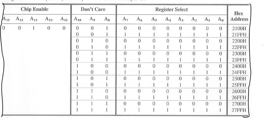
The address lines A10, A9, and A8 are not connected, thus they are left as don’t care lines.
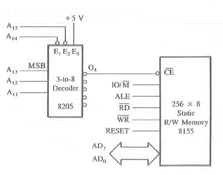
Figure 2 Interfacing circuit between the microprocessor and 8155 memory chip.
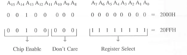
Thus the memory addresses of the 8155 memory will range from 2000H to 20FFH as follows:
In reality, the memory section of this 8155 uses the memory space from 2000H to 27FFH.
In figure 2 the address lines A10, A9, and A8 are not connected; thus they are don’t care lines capable of assuming any logic state 0 or 1.
Three don’t care address lines can be assumed to have any one of the eight combinations from 000 to 111. Thus each combination can generate one set of complete addresses.
The address range given by assuming all don’t care lines at logic 0 is, by convention, specified as the memory address range of the memory chip; the remaining address ranges are known as either foldback memory or mirror memory.
In this example, the primary address range is 2000H to 20FFH and the foldback memory range is 2100H to 27FFH.
Author of this post
This post is co-authored by Professor Saraswati Saha, who is an assistant professor at RCCIIT, a renowned degree engineering college in India. Professor Saha teaches subjects related to digital electronics & microprocessors.