
The Timing Diagram of INR M instruction of 8085
This post covers the Timing Diagram of INR M instruction of 8085. To understand the timing diagram, we first discussed the three machine cycles of INR M instruction.
INR M is a one-byte instruction available in the 8085 microprocessor instruction set. The Hex code for this instruction is 34H; therefore the instruction will be stored in a single memory address. It is used to increment the content of a memory location.
The content present in the designated memory location (M) cannot be changed in the memory location itself. It has to be read into the processor and then incremented by 1 and the modified result has to be written into the same memory address.
Note: If the operand is a memory location, it is specified by the contents of the HL pair.
Before discussing the timing diagram, let’s understand the machine cycles of INR M.
Three machine cycles of INR M instruction
INR M is a one-byte instruction and this instruction requires three machine cycles.
Machine Cycle1: Opcode Fetch
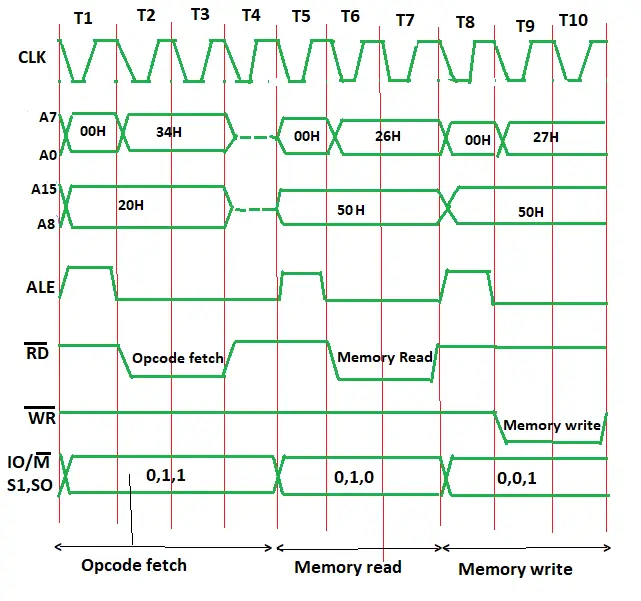
During this cycle, the opcode is fetched from the memory location. In this example, the opcode 34H is fetched from the location 2000H. Opcode fetch will take place during the first 4 T states (T1 to T4).
Machine Cycle2: Memory Read
In this instruction, M is the memory register and the address of this register is saying 5000H. Suppose the data present at M (or 5000H) is 26H.
So during the second machine cycle, the contents of the HL register pair (here it is 5000H)are placed in the address bus, the memory content (here it is 26H) is brought to the processor, and its value is incremented. The memory read operation will take place during the next 3 T states (T5 to T7).
Machine Cycle3: Memory Write
During the third machine cycle, the incremented data (here it is 27H) is again written back into the same address (here it is 5000H). Memory Write needs to be added in the successive 3 T states (T8 to T10).
Condition of the control and status signals during the execution of INR M instruction
For the opcode fetch the IO/M ‘ = 0, S1 = 1 and S0 = 1. RD’=0
For the memory read the IO/M ‘ = 0, S1 = 1 and S0 = 0. RD’=0
For the memory write the IO/M’ = 0, S1 = 0 and S0 = 1,WR’=0
ALE (Address Latch Enable) pin becomes HIGH only during the first T-states of each machine cycle to provide the signal for multiplexed address and data bus and the bus is used as the address bus to fetch the lower byte of the address. Otherwise, it will be used as a data bus.
The timing diagram of INR M instruction
The timing diagram of INR M instruction is shown below:
Author of this post
This post is co-authored by Professor Saraswati Saha, who is an assistant professor at RCCIIT, a renowned degree engineering college in India. Professor Saha teaches subjects related to digital electronics & microprocessors.