
Demultiplexing of Address Data bus in 8086
In this post, we will discuss Demultiplexing of Address/Data buses in an 8086 Processor.
Multiplexing is an important technique used for transferring different information at different times through the same lines. A group of such lines is called a multiplexed bus line. The result of multiplexing is that fewer pins are required for microprocessors to communicate with the external world.
Due to pin number limitations, most microprocessors cannot provide dedicated lines (such as address, data, status signals, etc.). Hence multiplexing of one or more of these buses is performed.
Most often data buses are multiplexed with some or all address buses to form an address /data bus (e.g., in 8086, the lower 16-address lines are multiplexed with data lines termed as AD0 to AD15). The status signals emitted by the microprocessor are sometimes multiplexed either with the data lines or with some of the address lines (as done in INTEL 8086).
Whenever multiplexing is used, the CPU interface of the system must include the necessary hardware to demultiplex those lines to produce separate address, data, and status lines required for the system.
Demultiplexing of Address/Data buses in an 8086 Processor
In order to demultiplex the address/data lines (of the processor), the processor provides a signal called ALE (Address Latch Enable). The ALE is asserted high and then low by the processor at the beginning of each machine cycle. At the same time, the address is given out through AD0 – AD15 lines and A16 – A19 /status lines.
Demultiplexing of address/data lines and address/status lines using 8-bit D-latch (IC 74LS373) is shown in Figure 1.
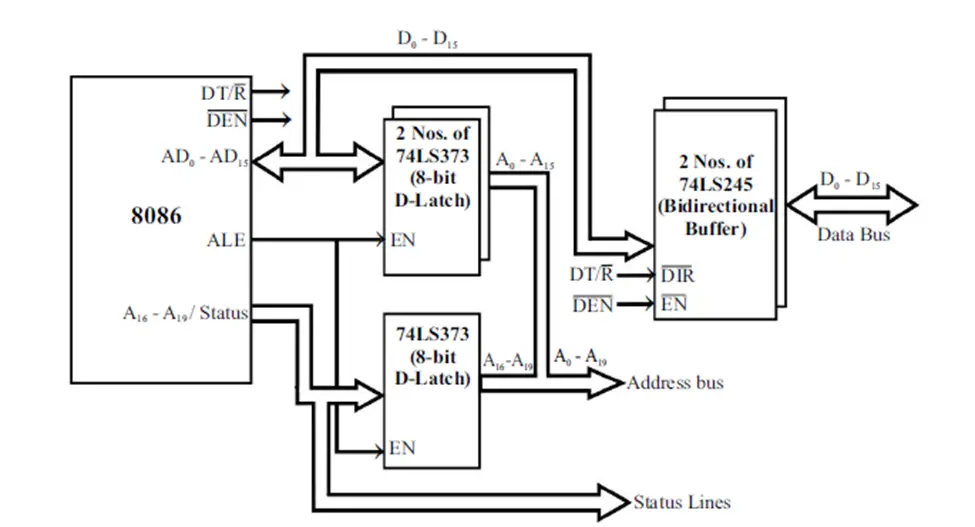
The ALE is connected to the Enable Pin (EN) of the external 8-bit latches.
When ALE is asserted high and then low, the addresses are latched into the output lines of the latch. It holds the address until the next machine cycle. After latching the address, the AD0 – AD15 lines are free for data transfer, and A16 – A19 /status lines are free for carrying status information.
The first T-state of each machine cycle is used for address latching in 8086 and the remaining T-states are used for reading operation or writing operation.
The data bus is buffered using two bidirectional buffers (IC74LS245) in order to drive the data to a longer distance in the bus.
The 8086 provides two control signals DT/R’(Data transmit/receive) and DEN’(Data bus enable) for controlling the data buffers.
If DEN’ is low, it indicates that the data is available on the multiplexed address/data bus (AD0-AD15). Both the bidirectional buffers are enabled to transfer that data since their enable inputs are activated at that time. The DT/R’ is used to decide the direction of data i.e. from/to the microprocessor, respectively.
Author of this post
This post is co-authored by Professor Saraswati Saha, who is an assistant professor at RCCIIT, a renowned degree engineering college in India. Professor Saha teaches subjects related to digital electronics & microprocessors.