
BCD Adder Design
In this post, we are going to discuss BCD Adder Design steps.
A BCD adder is a circuit that adds two BCD digits in parallel and produces a sum digit which is also in BCD. A BCD adder must include the correction logic (i.e. add 6 command) in its internal construction.
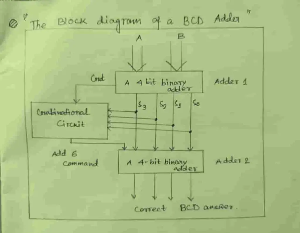
A block diagram for the BCD adder is shown in figure1. The block diagram shows that the BCD adder contains two 4-bit binary adders and one combinational logic circuit. This combinational circuit is used to generate the add 6 command.
Characteristics of a BCD Adder
A BCD adder circuit must be able to do the following:
- Add two BCD numbers using straight binary addition.
- If the Sum<=9 and carry=0, the sum is in proper BCD form and no correction is needed.
- If the Sum > 9 or if a carry=1, the sum is not in proper BCD form. Then, correction is required and the digit 6(0110) should be added to the sum to produce the BCD results. The carry may be produced due to this addition and it is added to the next decimal position.
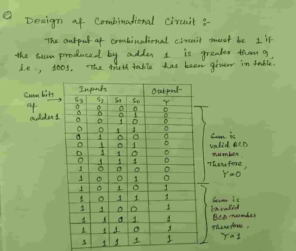
Design of combinational circuit to generate add 6 command
To design a combinational circuit first draw the truth table for it. Figure 2 shows the truth table. The inputs for the circuit are S3S2S1S0 of adder-1 and Y is the output. Output remains 0 till the Sum<=9 and carry=0 and Y=1 for Sum > 9 or if a carry=1.
Now solve the K-map for output Y which is shown in figure 3.
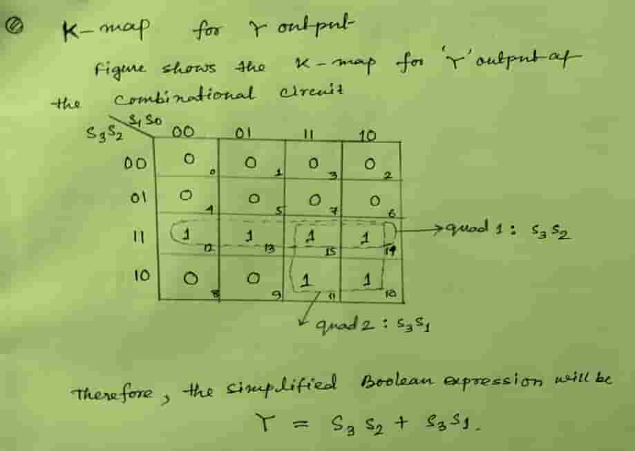
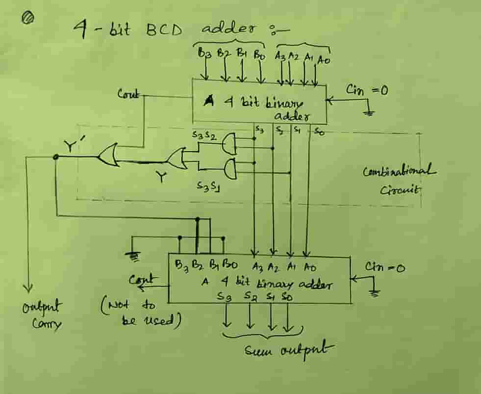
Now from the K-map, it is clear that the output (Y) of the combinational circuit is Y= S3S2 + S3S1, and carry of adder-1 (Cout) is again OR-ed with the output Y to generate the final output Y’.
Therefore, the condition for correction can be written as an expression as follows: Y’ = S3S2 + S3S1 + Cout So the corrected BCD adder circuit is shown in Figure 4.
Working operation of BCD adder
The circuit diagram of a BCD adder shows that the output of the combinational circuit must be 1 if Cout of adder-1 is high. Therefore, Y is OR-ed with Cout of adder 1 as shown in figure 4.
The output of combinational circuit Y’ is then connected to B2B1 inputs of adder-2 and B3=B1=0 as they are connected to the ground permanently. This makes B3B2B1B0=0110 if Y’=1.The sum outputs of adder-1 are applied to A3 A2 A1 A0 of adder-2.
The output of the combinational circuit is to be used as the final carry output and the carry output of adder-2 is to be ignored.
Then the operation of a BCD adder shown in Figure 4 is explained as follows: the first stage of the adder adds two 4-bit BCD numbers, and its sum (S3S2S1S0) and carry (Cout) are checked for the following cases.
CASE-I: Sum<=9 and carry=0
The output of combinational circuit Y’=0. Hence, B3B2B1B0=0000 for adder-2. Therefore, the output of adder-2 is the same as that of adder-1.
CASE-II: Sum > 9 and carry=0
S3S2S1S0 of adder-1 is greater than 9, and then the output Y of the combinational circuit becomes 1. Therefore, B3B2B1B0=0110 (of adder-2). Hence, six (0110) will be added to the sum output of adder-1. We get the corrected BCD result at the output of adder-2.
CASE-III: Sum <=9 but carry=1
As the carry output of adder-1 is high, we have, Y’=1. Therefore, B3B2B1B0=0110(of adder-2)
Hence, 0110 will be added to the sum output of adder-1. We get the corrected BCD result at the output of adder-2. Thus, the four bit BCD addition can be carried out using the binary adder.
Author of this post
This post is co-authored by Professor Saraswati Saha, who is an assistant professor at RCCIIT, a renowned degree engineering college in India. Professor Saha teaches subjects related to digital electronics & microprocessors.