
Full Adder Using 4×1 Multiplexers
Last updated on August 10th, 2023 at 05:07 am
The topic of this post is Full Adder Using 4×1 Multiplexers. This is searched as Full Adder Using Mux as well.
A full adder circuit is a combinational logic circuit that performs the addition of three bits and produces the Sum and Carry as an output. We are going to focus on building the full adder circuit using 4×1 Multiplexers. This multiplexer (mux) is also referred to as a 4:1 multiplexer.
But for a better understanding of the reader first, we will explain how the full adder is implemented using basic logic gates (K-Map solution) and then by the design table solution method.
- What is Full Adder?
- Block diagram of a Full Adder
- Truth Table of a Full Adder
- Combinational circuit from the truth table of a full adder
- Logic Diagram of a Full Adder using basic logic gates
- Full Adder Using Mux | Full adder using 4:1 Multiplexers [Implementation]
- Logic circuit for the full adder using two 4:1 multiplexer
What is Full Adder?
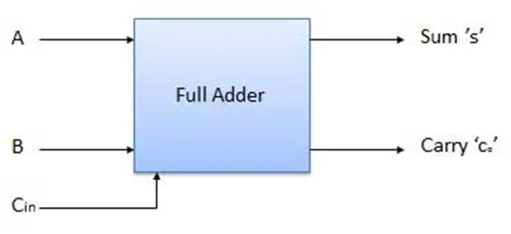
A full adder is a combinational logic circuit that performs the arithmetic sum of three bits. It consists of three inputs (each of one bit) termed as A, B, and Cin. Two inputs A and B, represent the two significant bits to be added. The third input, Cin, represents the carry from the previous lower significant position.
Two outputs are necessary because the arithmetic sum of three binary digits ranges in value from 0 to 3, and in binary 2 or 3 needs two digits.
Two outputs are designated by the symbols: ‘S ‘for sum and ‘Co’ for carry.
Block Diagram and the Truth Table of Full Adder
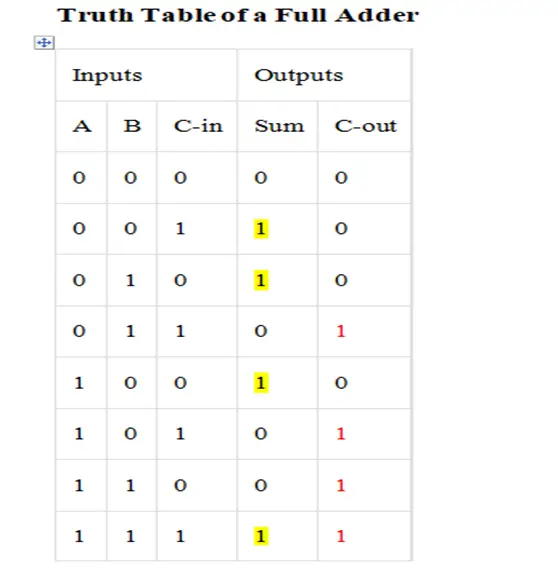
The block diagram and the truth table of a Full Adder are shown in Figure 1 and Figure 2.
Block diagram of a Full Adder
A truth table is written by the concept of binary addition. That is,

Truth Table of a Full Adder
Combinational circuit from the truth table of a full adder
From the truth table, a combinational circuit that will produce the correct sum and carry bits in response to every possible combination of A, B, and Cin is described below in the following steps.
Step 1: From the truth table write the expressions for the output SUM and CARRY in Sum of product (SOP) form.
For Sum – SUM (A, B, C-in) = Σ (1, 2, 4, 7)
For Carry- CARRY (A, B, C-in) = Σ (3, 5, 6, 7)
K-Map for SUM and CARRY output of a Full Adder
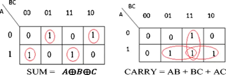
From K-Map, we will get

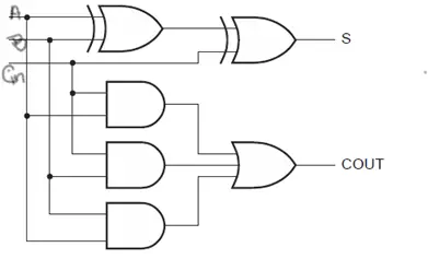
From the above expression, we can draw the logic diagram of a full adder.
Logic Diagram of a Full Adder using basic logic gates
Full Adder Using Mux | Full adder using 4:1 Multiplexers [Implementation]
From the above discussion, it is clear that the full adder circuit has three input terminals A, B, and Cin. So to implement the sum or carry functions using a 4:1 Multiplexer, two input variables B and C will be connected to the two select inputs S1 and S0 of the 4:1 multiplexer.
Now for the connection of the most significant bit (which is represented by the input variable A) to the inputs of the Multiplexer, the design table solution must be included in this design procedure.
Now solve the Design Table for Sum and Carry outputs for a full adder using two 4:1 multiplexers.
Design Table for Sum Output:
The size of the multiplexer is 4×1, so there are four input terminals D0 to D3. In the design table, there will be two rows, one for A’ and another for A, and four columns marked from D0 to D3.
Here the design table consists of 8 boxes and we have entered the decimal numbers corresponding to the minterms 0 to 7 serially. Encircle those minterms corresponds to an output=1
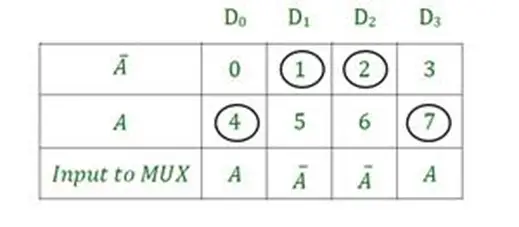
For sum output, the Minterms (1, 2, 4, 7) outputs are HIGH so they are circled in the design table.
The data inputs D0 to D3 have been written at the top of the table and the two possible values A’ and A to the left of two rows.
- For D0 only 4 is HIGH which corresponds to A in the table, So the D0 input for the MUX(M0) will be A.
- The same rule follows for the other inputs – D1=A’, D2=A’, D3=A.
Design Table for the Carry Output:
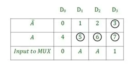
For Carry output the Minterms (3, 5, 6, 7) outputs are HIGH, so they are circled in the design table, just like the design table for sum.
- Here for the D0 input 0 and 4, both are LOW, so input to the MUX will be 0
- For D3 both 3 and 7 are HIGH, so the input to MUX will be 1.
- D1 and D2 will follow the previous rule and will be D1=A and D2=A
Now we have all the input information to the MUX, so we can design the logic circuit for the full adder using two 4:1 multiplexers.
Logic circuit for the full adder using two 4:1 multiplexer
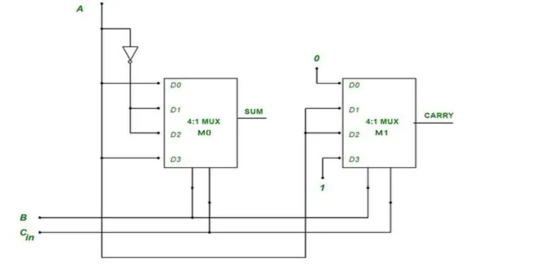
Summary of the circuit connection
For Inputs – The input to the M0 MUX is as per the design table of SUM i.e. D0 = A, D1 = A’, D2 = A’, D3 = A.
The input to the M1 MUX is as per the design table of CARRY i.e. D0 = 0, D1 = A, D2 = A, D3 = 1.
The selection lines S1 and S0 of both M0 and M1 are connected with the B & Cin input respectively.
For Outputs –
The output of M0 MUX will have the SUM as output and M1 MUX will have CARRY as output.
You can also go through this post:
Implementation of Boolean function using multiplexer
Author of this post
This post is co-authored by Professor Saraswati Saha, who is an assistant professor at RCCIIT, a renowned degree engineering college in India. Professor Saha teaches subjects related to digital electronics & microprocessors.