
The Architecture of 8085 and 8086 – Questions & answers
In this post, we will answer a bunch of selected questions on the architecture of 8085 and 8086 microprocessors.
After reading this article students will get an overall idea about the question pattern and the answer tips. This will also help the students with the self-study on 8085 and 8086 architecture.
- What is meant by instruction pipelining in 8086 microprocessor?
- What is the difference between the Minimum and Maximum mode operation of the 8086?
- What is memory segmentation?
- Identify the difference between Memory-mapped I/O and Peripheral-mapped I/O scheme.
- What is meant by Direct Memory Access (DMA) operation in a microprocessor?
- What is meant by Interrupt Driven data transfer scheme in a microprocessor?
- What is meant by Processor Status Word (PSW) or Program Status Word in a microprocessor?
- List the Segment Registers available in 8086 microprocessor and their function.
- What is meant by Status and control flags in the 8086 processor?
- Write the difference between maskable and non-maskable interrupts.
- Write the difference between software and hardware interrupts.
- Define the term Interrupt service routine (ISR) and interrupt vector address.
What is meant by instruction pipelining in 8086 microprocessor?
The 8086 architecture has a 6-byte instruction queue. Thus even the largest (6-bytes) instruction can be pre-fetched from the memory and stored in the pre-fetch queue. This results in faster execution of the instructions.
In the 8085 microprocessor, an instruction (opcode and operand) is fetched, decoded, and executed, and only after the execution of this instruction, the next one is fetched. But in the 8086 microprocessor, by pre-fetching the instruction, there is a considerable speeding up in instruction execution in 8086. This scheme is known as instruction pipelining.
What is the difference between the Minimum and Maximum mode operation of the 8086?
In the minimum mode, the 8086 microprocessor is operated by strapping its MN/MX’ pin to logic 1. In this mode, all the control signals are given out by the microprocessor chip itself. There is a single microprocessor in the minimum mode system. The remaining components in the system are latches, transceivers, clock generators, memory, and I/O devices.
In the maximum mode, the 8086 microprocessor is operated by strapping its MN/MX’ pin to the ground. In this mode the processor derives the status signals S2, S1 and S0. Another chip called the bus controller derives the control signals using this status information. In the maximum mode, there may be more than one microprocessor in the system configuration. The other components in the system are the same as in the minimum mode system.
What is memory segmentation?
Segmentation is the process in which the main memory of the computer is logically divided into different segments and each segment has its own base address. It is basically used to enhance the speed of execution of the computer system so that the processor is able to fetch and execute the data from the memory easily and fast.
Identify the difference between Memory-mapped I/O and Peripheral-mapped I/O scheme.
There are generally two addressing schemes for I/O devices in a microprocessor-based system.
(a) Memory-mapped I/O and (b) Peripheral-mapped I/O (I/O mapped I/O).
In a memory-mapped I/O scheme, an I/O device is treated as a memory- location, so an address is assigned to it (one address for each I/O device). In a memory-mapped I/O scheme, all data transfer instructions of the microprocessor, are applicable to memory as well as I/O devices.
In I/O mapped I/O scheme, I/O devices are treated as distinct from memory devices. The address, on the address bus, may refer either to a memory location or to an I/O device that will be separated by the control signal I/O/M’.
For example, in 8085, input /output devices can have addresses in the range 00-FFH in I/O mapped I/O addressing scheme and 0000H to FFFFH in the memory-mapped I/O scheme.
What is meant by Direct Memory Access (DMA) operation in a microprocessor?
Direct Memory Access (DMA) data transfer scheme in a microprocessor is used for bulk data transfer from an I/O device to a memory device or vice versa. If programmed data transfer is employed in such cases, it becomes a time-consuming process because data is first transferred to Accumulator and then to the concerned device.
In the DMA data transfer scheme, data is directly transferred from I/O devices to RAM or from RAM to I/O devices without being routed through Accumulator. The microprocessor is made to relinquish control of data and address buses so that these can be used for the transfer of data between the devices.
A device known as a programmable DMA controller is used for this purpose.
What is meant by Interrupt Driven data transfer scheme in a microprocessor?
Interrupt Driven data transfer scheme is used when the I/O device is quite slow. In this scheme, when an I/O device wants to transfer data to the microprocessor, it sends an interrupt signal to the processor which may be processing some data at that time. After completing the current instruction, the processor saves the contents of the program counter (PC), Accumulator (ACC), and flag registers in the stack and enters into a subroutine (ISR) to transfer data from the device. When data transfer has been completed, the processor resumes the execution of the main program.
What is meant by Processor Status Word (PSW) or Program Status Word in a microprocessor?
In a microprocessor, the flag register and Accumulator are connected with the ALU. So the status of different flags gets affected by arithmetic and logical operation performed in ALU.
The content of the accumulator along with the status flag register is therefore called Processor Status Word (PSW) or Program Status Word.
List the Segment Registers available in 8086 microprocessor and their function.
The Bus Interface Unit (BIU) in 8086 architecture contains, four 16-bit special-purpose registers, called Segment Registers that support the memory segmentation scheme in the 8086 microprocessor.
- Code segment register (CS): is used for addressing memory location in the code segment of the memory, where the executable program is stored.
- Data segment register (DS): points to the data segment of the memory where the data is stored.
- Extra Segment Register (ES): also refers to a segment in the memory which is another data segment in the memory.
- Stack Segment Register (SS): is used for addressing the stack segment of the memory. The stack segment is that segment of memory that is used to store stack data.
What is meant by Status and control flags in the 8086 processor?
The flags in the flag register can be classified into status flags and control flags. The flags CY(carry flag), P(parity flag), AC(auxiliary carry flag), Z (zero flag), S(sign flag), and O(overflow flag) are called status flags, as they indicate the status of the result that is obtained after the execution of an arithmetic or logic instruction.
The flags D (direction flag), I(interrupt flag), and T (trap flag) are called control flags, as they control the operation of the CPU.
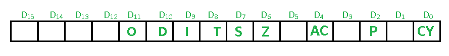
Fig.1 Flag register of the 8086
Write the difference between maskable and non-maskable interrupts.
- Maskable interrupts are interrupts that can be blocked; the corresponding ISRs are not executed. The masking can be done by software or hardware means. Example: RST7.5, RST6.5, and RST5.5 in 8085 processor.
- Non-maskable interrupts are interrupts that are always recognized; the corresponding ISRs are executed. Example TRAP in 8085.
Write the difference between software and hardware interrupts.
- Software interrupts are special instructions that after execution transfer the control to a predefined ISR. These instructions are included in the program by the programmer. Example: RST0 to RST7 in 8085 processor.
- Hardware interrupts are signals given to the processor, for recognition as an interrupt and execution of the corresponding ISR. Example: TRAP RST7.5, RST6.5, RST5.5, and INTR in 8085 processor.
Define the term Interrupt service routine (ISR) and interrupt vector address.
Interrupt service routine (ISR): The program or the routine that is executed upon interrupt is called interrupt service routine (ISR).
Interrupt vector address: The address of the memory where the ISR is located for a particular interrupt signal is called the interrupt vector address.
Author of this post
This post is co-authored by Professor Saraswati Saha, who is an assistant professor at RCCIIT, a renowned degree engineering college in India. Professor Saha teaches subjects related to digital electronics & microprocessors.