
Flip flop
Last updated on June 29th, 2023 at 02:13 pm
In this post, we will cover flip flop and different aspects of it, like types of flip flop, logic symbols, truth table, and applications of flip flop.
The basic building block for sequential logic circuits is the flip flop.
Logic circuits are classified into two groups. One is combination logic circuits using AND, OR, and NOT gates. The other group of circuits is classified as sequential logic circuits. Sequential circuits involve timing and memory devices.
The basic building block for sequential logic circuits is the flip flop (FF) whereas the basic building block for combinational logic circuits is the logic gate.
Types of flip flop
Flip-flops are different types depending on how their inputs and clock pulses cause a transition between the two states. There are four basic types, namely SR, JK, D, and T Flip flops.
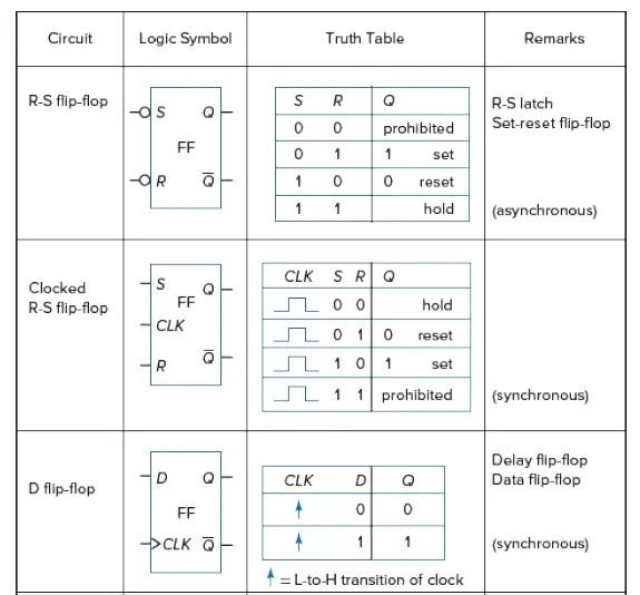
Logic symbols and Truth Tables of basic flip flops
Here are the logic symbols and truth table of basic flip-flops: shown in Table 1 and Table 2.
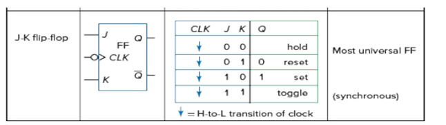
For the T flip flop the logic symbol is the same as the JK flip flop. The J and K inputs are wired together and named T input (As shown in Table 3)
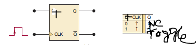
Table 3: Logic symbols and truth table of T flip-flop [ NC stands for No change ]
The knowledge of the logic symbols and truth table of basic flip flops are an important part to draw the logic diagram and understand the basic operation of any kind of sequential circuit.
If we see the logic symbols of different flip-flops, we can understand the variation in symbols used for clock input.
In the case of clocked RS flip flop (ref. Table 1), a clock symbol is used for the positive level triggering. For D and T flip flops (ref. table 1 and 3), the clock symbol represents the positive-edge triggering. For the JK flip flop (ref. Table 2), the clock symbol represents the negative-edge triggering.
Edge triggering of flip flop
The term edge-triggered means that the flip flop changes its state either at the positive edge (rising or leading edge) or at the negative edge (falling or trailing edge) of the clock pulse and is sensitive to its inputs only at this transition of the clock.
Difference between positive and negative edge triggering
The difference between positive and negative edge triggering can be explained in the following section with an example. ( D flip-flop with Positive-edge-triggered and Negative-edge-triggered clock signal )
D flip flop with Positive-edge-triggered and Negative-edge-triggered clock signal
The logic symbol for a D flip-flop with positive-edge triggering is shown in Fig. 1(a). Note the use of the small > inside the flip-flop logic symbol near the clock input. This > symbol says data are transferred to the output on the edge of the pulse.
A logic symbol for a D flip flop using negative-edge triggering is shown in Fig. 1(b). The added invert bubble at the clock input shows that triggering occurs on the negative-going edge (1 to 0 transition)of the clock pulse.
Finally, a typical D latch symbol is shown in Fig. 1(c). Note the lack of a > symbol next to the enable (similar to a clock) input shows that triggering occurs on the logic high level of the clock pulse.
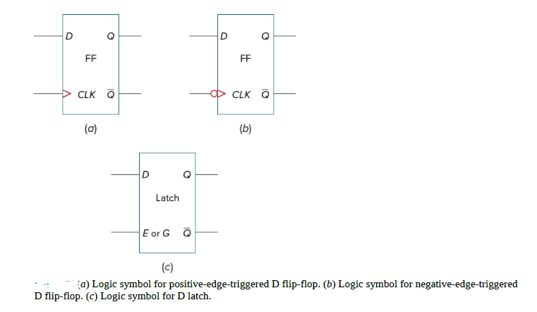
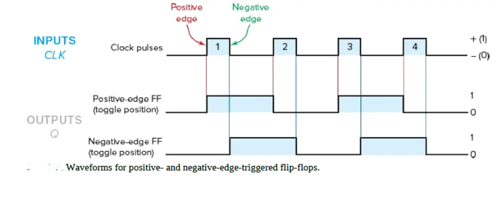
Figure 2: Waveforms for positive- and negative-edge-triggered D flip flop in toggle position.
Applications of Flip Flops
Flip-Flops find wide applications in counter circuits, frequency dividers, shift registers, and storage registers.
Author of this post
This post is co-authored by Professor Saraswati Saha, who is an assistant professor at RCCIIT, a renowned degree engineering college in India. Professor Saha teaches subjects related to digital electronics & microprocessors.