8255 PPI Programmable Peripheral Interface
Last updated on May 9th, 2022 at 01:45 pm
In this post, we will discuss the 8255 PPI Programmable Peripheral Interface and find answers to a bunch of interesting questions on this.
What is 8255 PPI?
8255 programmable peripheral interface (PPI) is a popularly used parallel, programmable input-output device. It can be used to transfer data between external devices (such as input and output devices) and the Intel 8085 microprocessor.
What do you mean by 8255 PPI?
PPI 8255 is a general-purpose programmable I/O (input/output) device designed to interface the CPU (central processing unit) with its outside world such as ADC (Analog to digital), DAC (Digital to analog), keyboard, etc.
It consists of three 8-bit bidirectional I/O ports i.e. PORT A, PORT B, and PORT C. We can assign different ports as input or output operations.
What is the use of 8255?
PPI 825 IC is an economical, functional, and flexible I/O (input/output) device that can be used with almost any microprocessor to interface with its outside world such as ADC (Analog to digital converter), DAC (Digital to analog converter), keyboard, etc.
The common applications of the 8255 with the 8085 include
- sensing a switch
- controlling movement by use of motors
- detecting a position
What are the features of 8255 PPI?
Each 8255 has three 8-bit TTL compatible registers or ports (such as PORT-A, PORT-B, PORT-C), which allow programmers to control digital outputs, inputs, or a combination of both.
The common features of Intel 8255 IC are as follows:
- It consists of 40 pins and operates in +5V regulated power supply.
- It consists of three 8-bit bidirectional I/O ports i.e. PORT A, PORT B and PORT C.
- Port C is further divided into two 4-bit ports i.e. port C lower (PCL) and port C upper (PCU). Each of them can be programmed independently in BSR (bit set rest mode) or as 4-bit ports, for input and output mode of 8255.
- Port B can work in either mode0 (simple I/O mode) or in mode 1(Handshake I/O mode) of input/output mode.
- Port A can work either in mode 0(simple I/O mode), mode 1(Handshake I/O mode) or mode 2 (Bidirectional I/O mode) of input-output mode.
- It has two control groups, control group A and control group B. Control group A (GA) consist of Port A and PCU. Control group B (GB) consists of port C lower (PCL) and port B.
Pin diagram, allocation of pins for different signals in the IC 8255 PPI – describe.
8255 programmable peripheral interface (PPI) is a popularly used parallel, programmable input-output device. It consists of 40 pins and operates in a +5 V regulated power supply. Pin diagram of 8255PPI is shown below:
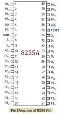
Figure 1: Pin Diagram of 8255 PPI
Table: Pin allocation for different signal pins
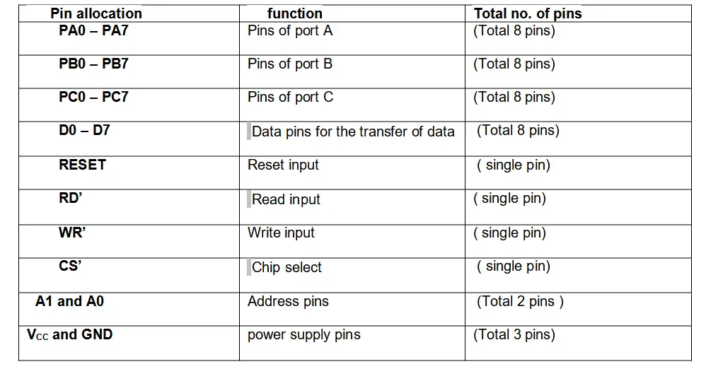
Summary of pin functions of IC 8255 PPI
The three ports of the 8255 need 8 lines each. So 24 pins (PA0 – PA7, PB0 – PB7 & PC0 – PC7) are allotted for the ports and these lines are connected to external input and output devices.
D0 – D7 (8 lines) are the lines required for interfacing the 8255 with the processor. These data lines are connected to the data bus of the processor.
Eight lines or pins are remaining. Out of these 8 lines, two lines- A1 and A0 are allotted for selecting one of the four registers available in the 8255.
The control signals (RD’ & WR’) are used for reading (from the registers) and writing into the registers, are the active lows. RD’ & WR’ signals are obtained from the processor’s control signals.
The active-low chip select (CS’) signal is used to select chip 8255. This signal is obtained from the decoder, which decodes the 8085 address lines and identifies the 8255 address range.
A common reset signal such as the RESET OUT of the 8085 processor can be applied to reset the 8255. For this purpose, the RESET pin is there in 8255.
Apart from these 38 pins, there are 2 pins for power supply connection, VCC and GND.
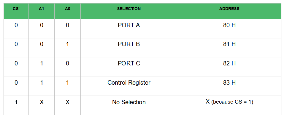
Explain how the different ports and control words are selected for 8255.
Depending upon the value of CS’, A1 and A0 we can select different ports in different modes as the input-output function or BSR. This is done by writing a suitable word in the control register (control word D0-D7).
The two address lines, along with the CS signal, determine the selection of a particular port or control register. This is explained below:
Address lines and register selection in 8255