
IC Packaging | Integrated Circuit Packaging
In this post, we will discuss IC Packaging or Integrated Circuit Packaging. In this process, we will also learn about the Dual-in-line package or DIP IC Package, and Surface Mount IC packages (SMT) packages.
IC Packaging | Integrated Circuit Packaging
A traditional type of IC is illustrated in Fig1(a). This case style is referred to as a dual in-line package (DIP) by IC manufacturers. This particular IC is called a 14-pin DIP IC.
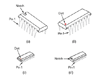
figure 1: Dual in-line package (DIP) ICs. Regular and micro size.
(a) Regular-size DIP- locating pin 1 using a notch. (b) Regular-size DIP-locating pin 1 using a dot. (c) Micro-size DIP surface mount IC locating pin 1 using a dot. (d) Micro size DIP surface-mount IC locating pin 1 using a notch.
Dual-in-line package | DIP IC Package
Just counterclockwise from the notch on the IC in Fig. (a) is pin 1. The pins are numbered counterclockwise from 1 to 14 when viewed from the top of the IC. A dot on the top of the DIP IC as in Fig.(b) is another method used to locate pin 1.
The ICs in Fig. (a) and (b) have longer pins that are commonly inserted through holes drilled in a printed circuit board and soldered to copper traces on the bottom. The two ICs in Fig.(c) and (d) are much smaller and have shorter pins bent to be soldered to the traces on the top of the PC board.
Surface mount IC packages
Surface mount IC packages – The smaller micro packages in Fig. (c) and (d) are commonly called surface-mount technology (SMT) packages. The SMT packages are typically much smaller in order to save PC board space and are easier to align when being positioned and soldered using automated manufacturing equipment. Two methods of locating pin 1 on the small SMT packages are illustrated in Fig.(c) and (d).
In your lab, you will probably use the larger DIP IC, which is shown in Fig.(a) with long pins because they can be inserted into a solder-less breadboard.