
IC Pin diagram & Wiring Diagram
In this post on Digital IC (Integrated Circuit), we will study the Pin diagram of a TTL IC. We will also take a Logic diagram for a two-input AND gate circuit and then come up with a Wiring diagram to implement the two-input AND function.
IC Pin diagram | Pin diagram of a TTL IC
Manufacturers of ICs provide pin diagrams similar to the one shown in figure 1. This IC contains 4 two-input AND gates. Thus, it is called a quadruple two-input AND gate.
This 7408 unit is one of many of the 7400 series of TTL ICs available. The power connections to the IC are the GND (pin 7) and VCC (pin 14) pins. All other pins are the inputs and outputs to the four TTL AND gates.
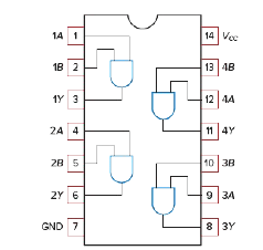
figure 1: Pin diagram for the 7408 digital IC.
IC Wiring Diagram | IC wiring diagram from a logic diagram
Given the logic diagram in Fig. 2 (a), let’s wire this circuit using the 7408 TTL IC.
A wiring diagram for the circuit is shown in Fig.2(b). A 5-V dc regulated power supply is typically used with TTL devices.
The positive (VCC) and negative (GND) power connections are made to pins 14 and 7 of the IC. Input switches (A and B) are wired to pins 1 and 2 of the 7408 IC. Notice that if a switch is in the up position, a logical 1 (+5 V) is applied to the input of the AND gate.
If a switch is in the down position, however, a logical 0 is applied to the input. At the right in Fig.(b), an LED and 150-Ω limiting resistor are connected to GND. If the output at pin 3 is HIGH (near +5 V), the current will flow through the LED. When the LED is lit, it indicates a HIGH output from the AND gate.
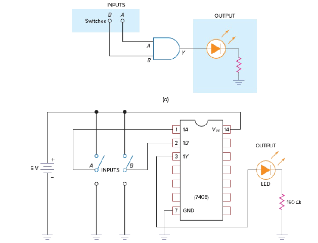
Fig. 2a) Logic diagram for a two-input AND gate circuit. (b) Wiring diagram to implement the two-input AND function.