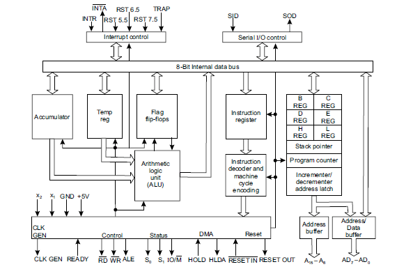
Functional block diagram of Intel 8085 microprocessor and the functional units
Last updated on March 5th, 2022 at 05:04 am
The 8085 is an 8-bit processor since its data length and data bus width are 8-bits. It has an addressing capability of 16 bits, that is, it can address 216=64 KB of memory. The 8085 processor is generally available as a 40-pin IC package and uses+5V for power. It can run at a maximum frequency of 3 MHz.
Functional block diagram of Intel 8085 microprocessor
The block diagram explaining the architecture of the Intel 8085 microprocessor is shown in the figure below.

Figure 1: Functional block diagram of Intel 8085 microprocessor
Various functional blocks of 8085 are as follows:
- Arithmetic and logic unit
- General-purpose registers
- Special- purpose registers
- Instruction register and decoder
- Timing and control unit
- Interrupt control
- Serial I/O control
Name the registers of 8085 microprocessor not accessible to the programmer
The following registers cannot be accessed by the programmer:
- Instruction register (IR)
- Memory address register (MAR)
- Temporary registers.
Does the ALU have any storage facility?
No, it does not have any storage facility. For this reason, the need for temporary data registers arises in ALU – it has two inputs: one provided by the accumulator and the other from the temporary data register. The result of summation is stored in the accumulator.
Related posts
Here are links to the articles we published on the Architecture of the 8085 microprocessor.
Functional block diagram of Intel 8085 microprocessor and the functional units
General-purpose registers of 8085 microprocessor
Special-purpose registers of 8085 microprocessor – FAQs
Different Signals used in 8085 microprocessor & their significance – FAQs
Author of this post
This post is co-authored by Professor Saraswati Saha, who is an assistant professor at RCCIIT, a renowned degree engineering college in India. Professor Saha teaches subjects related to digital electronics & microprocessors.
