Full-wave rectifier: circuit diagram, working principle & wave-forms
In this post, we will draw a circuit diagram of a full-wave rectifier and Explain its working principle. We will also draw the input & output wave-forms of a Full-wave rectifier indicating clearly the functions of the two diodes used.
Full Wave Rectifier: circuit diagram and working principle
For a full-wave rectifier, we use two junction diodes. The circuit diagram for a full-wave rectifier using two junction diodes is shown in figure 1.
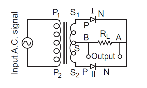
Suppose during the first half-cycle of the input ac signal the terminal S1 is positive relative to S and S2 is negative relative to S, then diode I is forward biased and diode II is reverse biased.
Therefore current flows in diode I and not in diode II. The direction of current i1 due to diode I in load resistance RL is directed from A to B.
In the next half-cycle, the terminal S1 is negative relative to S and S2 is positive relative to S. Then diode I is reverse biased and diode II is forward biased. Therefore current flows in diode II and there is no current in diode I. The direction of current i2 due to diode II in load resistance is again from A to B.
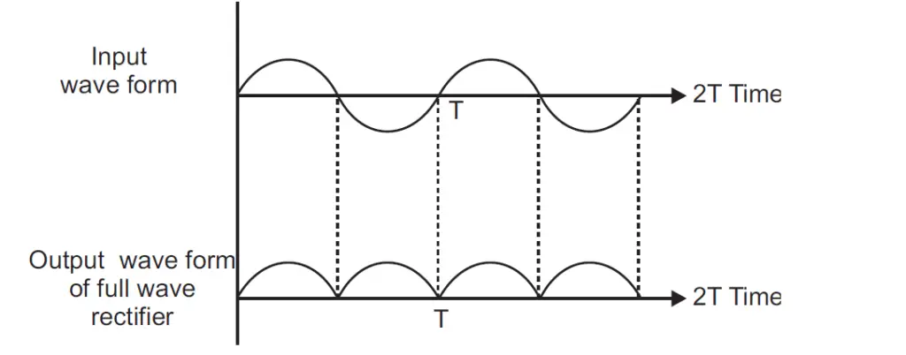
Thus for input a.c. signal the output current is a continuous series of unidirectional pulses (figure 2). This output current may be converted into a fairly steady current by the use of suitable filters.
Draw the input & output wave-forms of a Full Wave Rectifier
For input a.c. signal the output current is a continuous series of unidirectional pulses for a Full Wave Rectifier (figure 2).